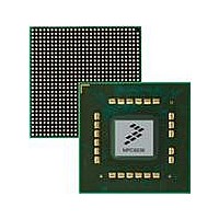
MPC8536DS Freescale Semiconductor, MPC8536DS Datasheet - Page 1075

MPC8536DS
Manufacturer Part Number
MPC8536DS
Description
BOARD DEV SYSTEM MPC8536E
Manufacturer
Freescale Semiconductor
Series
PowerQUICC III™r
Type
MPUr
Datasheets
1.MPC8536EBVTAVLA.pdf
(127 pages)
2.MPC8536EBVTAVLA.pdf
(1706 pages)
3.MPC8536DS.pdf
(2 pages)
4.MPC8536DS.pdf
(126 pages)
Specifications of MPC8536DS
Contents
Board, Software and Documentation
Processor Series
MPC85xx
Core
e500
Data Bus Width
32 bit
Maximum Clock Frequency
667 MHz
Operating Supply Voltage
- 0.3 V to + 1.21 V
Maximum Operating Temperature
+ 105 C
Data Ram Size
32 KB
Interface Type
SPI, USB
Program Memory Type
DDR2, DDR3, SDRAM
Core Size
32 Bit
Program Memory Size
544KB
Cpu Speed
1.5GHz
Digital Ic Case Style
BGA
No. Of Pins
783
Supply Voltage Range
0.95V To 1.05V
Rohs Compliant
Yes
For Use With/related Products
MPC8536
Lead Free Status / RoHS Status
Lead free / RoHS Compliant
- MPC8536EBVTAVLA PDF datasheet
- MPC8536EBVTAVLA PDF datasheet #2
- MPC8536DS PDF datasheet #3
- MPC8536DS PDF datasheet #4
- Current page: 1075 of 1706
- Download datasheet (15Mb)
A target must assert PCI_DEVSEL (claim the transaction) before or coincident with any other target
response (assert PCI_TRDY, PCI_STOP, or data signals). In all cases except target-abort, once a target
asserts PCI_DEVSEL, it must not negate PCI_DEVSEL until PCI_FRAME is negated (with PCI_IRDY
asserted) and the last data phase has completed. For normal termination, negation of PCI_DEVSEL
coincides with the negation of PCI_TRDY or PCI_STOP.
If the first access maps into a target’s address range, that target asserts PCI_DEVSEL to claim the access.
However, if the initiator attempts to continue the burst access across the resource boundary, then the target
must issue a target disconnect.
The PCI controller is hardwired for fast device select timing (PCI bus status register [10–9] = 0b00).
Therefore, when the PCI controller is the target of a transaction (local memory access or configuration
register access), it asserts PCI_DEVSEL one clock cycle following the address phase.
As an initiator, if the PCI controller does not detect the assertion of PCI_DEVSEL within four clock cycles
after the address phase (that is, five clock cycles after it asserts PCI_FRAME), it terminates the transaction
with a master-abort termination; see
16.4.2.5
The byte enable signals of the PCI bus (PCI_C/BE[3:0], during a data phase) are used to determine which
byte lanes carry meaningful data. The byte enable signals may enable different bytes for each of the data
phases. The byte enables are valid on the edge of the clock that starts each data phase and stay valid for
the entire data phase. Note that parity is calculated for all bytes regardless of the state of the byte enable
signals. See
If the PCI controller, as a target, detects no byte enables asserted, it completes the current data phase with
no permanent change. This implies that on a read transaction, the PCI controller expects that the data is
not changed, and on a write transaction, the data is not stored.
16.4.2.6
To avoid contention, a turnaround cycle is required on all signals that may be driven by more than one
agent. The turnaround cycle occurs at different times for different signals. The PCI_IRDY, PCI_TRDY,
PCI_DEVSEL, and PCI_STOP signals use the address phase as their turnaround cycle.
PCI_FRAME,PCI_C/BE[3:0], and PCI_AD[31:0] signals use the idle cycle between transactions (when
both PCI_FRAME and PCI_IRDY are negated) as their turnaround cycle. PCI_PERR has a turnaround
cycle on the fourth clock cycle after the last data phase.
The PCI address/data signals, PCI_AD[31:0], are driven to a stable condition during every address/data
phase. Even when the byte enables indicate that byte lanes carry meaningless data, the signals carry stable
values. Parity is calculated on all bytes regardless of the byte enables. See
Parity,”
Freescale Semiconductor
for more information.
Section 16.4.2.13.1, “PCI Parity,”
Byte Alignment
Bus Driving and Turnaround
MPC8536E PowerQUICC III Integrated Processor Reference Manual, Rev. 1
Section 16.4.2.8.1, “Master-Initiated Termination.”
for more information.
Section 16.4.2.13.1, “PCI
PCI Bus Interface
16-49
Related parts for MPC8536DS
Image
Part Number
Description
Manufacturer
Datasheet
Request
R
Part Number:
Description:
Manufacturer:
Freescale Semiconductor, Inc
Datasheet:
Part Number:
Description:
Manufacturer:
Freescale Semiconductor, Inc
Datasheet:
Part Number:
Description:
Manufacturer:
Freescale Semiconductor, Inc
Datasheet:
Part Number:
Description:
Manufacturer:
Freescale Semiconductor, Inc
Datasheet:
Part Number:
Description:
Manufacturer:
Freescale Semiconductor, Inc
Datasheet:
Part Number:
Description:
Manufacturer:
Freescale Semiconductor, Inc
Datasheet:
Part Number:
Description:
Manufacturer:
Freescale Semiconductor, Inc
Datasheet:
Part Number:
Description:
Manufacturer:
Freescale Semiconductor, Inc
Datasheet:
Part Number:
Description:
Manufacturer:
Freescale Semiconductor, Inc
Datasheet:
Part Number:
Description:
Manufacturer:
Freescale Semiconductor, Inc
Datasheet:
Part Number:
Description:
Manufacturer:
Freescale Semiconductor, Inc
Datasheet:
Part Number:
Description:
Manufacturer:
Freescale Semiconductor, Inc
Datasheet:
Part Number:
Description:
Manufacturer:
Freescale Semiconductor, Inc
Datasheet:
Part Number:
Description:
Manufacturer:
Freescale Semiconductor, Inc
Datasheet:
Part Number:
Description:
Manufacturer:
Freescale Semiconductor, Inc
Datasheet:


