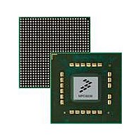
MPC8536DS Freescale Semiconductor, MPC8536DS Datasheet - Page 740

MPC8536DS
Manufacturer Part Number
MPC8536DS
Description
BOARD DEV SYSTEM MPC8536E
Manufacturer
Freescale Semiconductor
Series
PowerQUICC III™r
Type
MPUr
Datasheets
1.MPC8536EBVTAVLA.pdf
(127 pages)
2.MPC8536EBVTAVLA.pdf
(1706 pages)
3.MPC8536DS.pdf
(2 pages)
4.MPC8536DS.pdf
(126 pages)
Specifications of MPC8536DS
Contents
Board, Software and Documentation
Processor Series
MPC85xx
Core
e500
Data Bus Width
32 bit
Maximum Clock Frequency
667 MHz
Operating Supply Voltage
- 0.3 V to + 1.21 V
Maximum Operating Temperature
+ 105 C
Data Ram Size
32 KB
Interface Type
SPI, USB
Program Memory Type
DDR2, DDR3, SDRAM
Core Size
32 Bit
Program Memory Size
544KB
Cpu Speed
1.5GHz
Digital Ic Case Style
BGA
No. Of Pins
783
Supply Voltage Range
0.95V To 1.05V
Rohs Compliant
Yes
For Use With/related Products
MPC8536
Lead Free Status / RoHS Status
Lead free / RoHS Compliant
- MPC8536EBVTAVLA PDF datasheet
- MPC8536EBVTAVLA PDF datasheet #2
- MPC8536DS PDF datasheet #3
- MPC8536DS PDF datasheet #4
- Current page: 740 of 1706
- Download datasheet (15Mb)
Enhanced Local Bus Controller
operation to the bank. At the conclusion of the sequence, eLBC will issue a command complete interrupt
(LTESR[CC]) if interrupts are enabled.
Note that operations specified by OP3 and OP4 (status read) should never be skipped while erasing a
NAND Flash device, because, in case that happens, contention may arise on LGPL4. A possible case is
that the next transaction from eLBC may try to use that pin as an output and since the NAND Flash device
might already be driving it, contention will occur. In case OP3 and OP4 operations are skipped, it may also
happen that a new command is issued to the NAND Flash device even when the device has not yet finished
processing the previous request. This may also result in unpredictable behavior.
13.5.4.6
An example of configuring FCM to execute a program command to large-page NAND Flash is shown in
Table
RAM, generating ECC as it proceeds. The shared buffer (buffer 1 for page index 5) must be initialized by
software prior to starting the sequence. The sequence is initiated by writing FMR[OP] = 11, and issuing a
special operation to the bank. At the conclusion of the sequence, eLBC will issue a command complete
interrupt (LTESR[CC]) if interrupts are enabled. The status of the programming operation is returned in
MDR[AS0].
Note that operations specified by OP5 and OP6 (status read) should never be skipped while programming
a NAND Flash device, because, in case that happens, contention may arise on LGPL4. A possible case is
that the next transaction from eLBC may try to use that pin as an output and since the NAND Flash device
might already be driving it, contention will occur. In case OP5 and OP6 operations are skipped, it may also
happen that a new command is issued to the NAND Flash device even when the device has not yet finished
processing the previous request. This may also result in unpredictable behavior.
13-98
13-49. This sequence writes an entire page (main and spare region) from the shared FCM buffer
Register
FBAR
FBCR
FPAR
MDR
FCR
FIR
NAND Flash Program Command Sequence Example
MPC8536E PowerQUICC III Integrated Processor Reference Manual, Rev. 1
Table 13-48. FCM Register Settings for Block Erase (OR n [PGS] = 1)
(e.g. block 0x00010AB4)
Initial Contents
0x426DB000
0x6070D000
0x00000000
block index
—
—
CMD0 = 0x60 = block address entry;
CMD1 = 0x70 = read status
CMD2 = 0xD0 = erase block;
BLK locates index of 128-Kbyte block
PI = 0 to locate block boundary
unused
returns with AS0 holding erase status
OP0 = CM0 = command 0;
OP1 = PA = page address;
OP2 = CM2 = command 2;
OP3 = CW1 = wait on Flash ready and issue command 1;
OP4 = RS = read erase status into MDR[AS0];
OP5–OP7 = NOP
Description
Freescale Semiconductor
Related parts for MPC8536DS
Image
Part Number
Description
Manufacturer
Datasheet
Request
R
Part Number:
Description:
Manufacturer:
Freescale Semiconductor, Inc
Datasheet:
Part Number:
Description:
Manufacturer:
Freescale Semiconductor, Inc
Datasheet:
Part Number:
Description:
Manufacturer:
Freescale Semiconductor, Inc
Datasheet:
Part Number:
Description:
Manufacturer:
Freescale Semiconductor, Inc
Datasheet:
Part Number:
Description:
Manufacturer:
Freescale Semiconductor, Inc
Datasheet:
Part Number:
Description:
Manufacturer:
Freescale Semiconductor, Inc
Datasheet:
Part Number:
Description:
Manufacturer:
Freescale Semiconductor, Inc
Datasheet:
Part Number:
Description:
Manufacturer:
Freescale Semiconductor, Inc
Datasheet:
Part Number:
Description:
Manufacturer:
Freescale Semiconductor, Inc
Datasheet:
Part Number:
Description:
Manufacturer:
Freescale Semiconductor, Inc
Datasheet:
Part Number:
Description:
Manufacturer:
Freescale Semiconductor, Inc
Datasheet:
Part Number:
Description:
Manufacturer:
Freescale Semiconductor, Inc
Datasheet:
Part Number:
Description:
Manufacturer:
Freescale Semiconductor, Inc
Datasheet:
Part Number:
Description:
Manufacturer:
Freescale Semiconductor, Inc
Datasheet:
Part Number:
Description:
Manufacturer:
Freescale Semiconductor, Inc
Datasheet:


