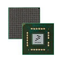
MPC8536DS Freescale Semiconductor, MPC8536DS Datasheet - Page 734

MPC8536DS
Manufacturer Part Number
MPC8536DS
Description
BOARD DEV SYSTEM MPC8536E
Manufacturer
Freescale Semiconductor
Series
PowerQUICC III™r
Type
MPUr
Datasheets
1.MPC8536EBVTAVLA.pdf
(127 pages)
2.MPC8536EBVTAVLA.pdf
(1706 pages)
3.MPC8536DS.pdf
(2 pages)
4.MPC8536DS.pdf
(126 pages)
Specifications of MPC8536DS
Contents
Board, Software and Documentation
Processor Series
MPC85xx
Core
e500
Data Bus Width
32 bit
Maximum Clock Frequency
667 MHz
Operating Supply Voltage
- 0.3 V to + 1.21 V
Maximum Operating Temperature
+ 105 C
Data Ram Size
32 KB
Interface Type
SPI, USB
Program Memory Type
DDR2, DDR3, SDRAM
Core Size
32 Bit
Program Memory Size
544KB
Cpu Speed
1.5GHz
Digital Ic Case Style
BGA
No. Of Pins
783
Supply Voltage Range
0.95V To 1.05V
Rohs Compliant
Yes
For Use With/related Products
MPC8536
Lead Free Status / RoHS Status
Lead free / RoHS Compliant
- MPC8536EBVTAVLA PDF datasheet
- MPC8536EBVTAVLA PDF datasheet #2
- MPC8536DS PDF datasheet #3
- MPC8536DS PDF datasheet #4
- Current page: 734 of 1706
- Download datasheet (15Mb)
Enhanced Local Bus Controller
13.5.1.3
In case a system contains a memory hierarchy with high speed synchronous memories (synchronous
SRAM) and lower speed asynchronous memories (for example, FLASH EPROM and peripherals) the
GPCM-controlled memories should be decoupled by buffers to reduce capacitive loading on the bus.
Those buffers have to be taken into account for the timing calculations.
To calculate address setup timing for a slower peripheral/memory device, several parameters have to be
added: propagation delay for the address latch, propagation delay for the buffer and the address setup for
the actual peripheral. Typical values for the two propagation delays are in the order of 3–6 ns, so for a
133-MHz bus frequency, LCS should arrive on the order of 3 bus clocks later.
For data timings, only the propagation delay of one buffer plus the actual data setup time has to be
considered.
13.5.2
Because the local bus uses multiplexed address and data, special consideration must be given to avoid bus
contention at bus turnaround. The following cases must be examined:
The bus does not change direction for the following cases so they need no special attention:
13-92
•
•
•
•
•
Address phase after previous read
Read data phase after address phase
Read-modify-write cycle for parity protected memory banks
UPM cycles with additional address phases
Continued burst after the first beat
Bus Turnaround
GPCM Timings
Local Bus Interface
Local Bus Interface
MPC8536E PowerQUICC III Integrated Processor Reference Manual, Rev. 1
LAD[0:31]
LAD[0:31]
LBCTL
LBCTL
LALE
Figure 13-73. GPCM Address Timings
Figure 13-74. GPCM Data Timings
Muxed Address/Data
Latch
Buffered Data
Buffer
A
Buffer
Muxed Address/Data
Unmuxed Address
Buffered Address
A
D
Device
Input
Device
Pin
Input
Pin
Peripherals
Memories
Peripherals
Memories
Slower
Slower
Freescale Semiconductor
and
and
Related parts for MPC8536DS
Image
Part Number
Description
Manufacturer
Datasheet
Request
R
Part Number:
Description:
Manufacturer:
Freescale Semiconductor, Inc
Datasheet:
Part Number:
Description:
Manufacturer:
Freescale Semiconductor, Inc
Datasheet:
Part Number:
Description:
Manufacturer:
Freescale Semiconductor, Inc
Datasheet:
Part Number:
Description:
Manufacturer:
Freescale Semiconductor, Inc
Datasheet:
Part Number:
Description:
Manufacturer:
Freescale Semiconductor, Inc
Datasheet:
Part Number:
Description:
Manufacturer:
Freescale Semiconductor, Inc
Datasheet:
Part Number:
Description:
Manufacturer:
Freescale Semiconductor, Inc
Datasheet:
Part Number:
Description:
Manufacturer:
Freescale Semiconductor, Inc
Datasheet:
Part Number:
Description:
Manufacturer:
Freescale Semiconductor, Inc
Datasheet:
Part Number:
Description:
Manufacturer:
Freescale Semiconductor, Inc
Datasheet:
Part Number:
Description:
Manufacturer:
Freescale Semiconductor, Inc
Datasheet:
Part Number:
Description:
Manufacturer:
Freescale Semiconductor, Inc
Datasheet:
Part Number:
Description:
Manufacturer:
Freescale Semiconductor, Inc
Datasheet:
Part Number:
Description:
Manufacturer:
Freescale Semiconductor, Inc
Datasheet:
Part Number:
Description:
Manufacturer:
Freescale Semiconductor, Inc
Datasheet:


