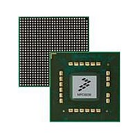
MPC8536DS Freescale Semiconductor, MPC8536DS Datasheet - Page 253

MPC8536DS
Manufacturer Part Number
MPC8536DS
Description
BOARD DEV SYSTEM MPC8536E
Manufacturer
Freescale Semiconductor
Series
PowerQUICC III™r
Type
MPUr
Datasheets
1.MPC8536EBVTAVLA.pdf
(127 pages)
2.MPC8536EBVTAVLA.pdf
(1706 pages)
3.MPC8536DS.pdf
(2 pages)
4.MPC8536DS.pdf
(126 pages)
Specifications of MPC8536DS
Contents
Board, Software and Documentation
Processor Series
MPC85xx
Core
e500
Data Bus Width
32 bit
Maximum Clock Frequency
667 MHz
Operating Supply Voltage
- 0.3 V to + 1.21 V
Maximum Operating Temperature
+ 105 C
Data Ram Size
32 KB
Interface Type
SPI, USB
Program Memory Type
DDR2, DDR3, SDRAM
Core Size
32 Bit
Program Memory Size
544KB
Cpu Speed
1.5GHz
Digital Ic Case Style
BGA
No. Of Pins
783
Supply Voltage Range
0.95V To 1.05V
Rohs Compliant
Yes
For Use With/related Products
MPC8536
Lead Free Status / RoHS Status
Lead free / RoHS Compliant
- MPC8536EBVTAVLA PDF datasheet
- MPC8536EBVTAVLA PDF datasheet #2
- MPC8536DS PDF datasheet #3
- MPC8536DS PDF datasheet #4
- Current page: 253 of 1706
- Download datasheet (15Mb)
These effective PLRU bits are used to select a victim, as indicated in
6.9
This section describes the behavior of the L1 and L2 cache in response to various operations and in various
configurations.
6.9.1
6.9.1.1
After power-on reset the valid bits in the L2 cache status array are in random states. Therefore, it is
necessary to perform a flash invalidate before using the array as an L2 cache. This is done by writing a one
to the L2I field of the L2 control register (L2CTL). This can be done before or simultaneously with the
write that enables the L2 cache. That is, the L2E and L2I bits of L2CTL can be set simultaneously. The
L2I bit clears automatically, so no further writes are necessary.
6.9.1.2
After power-on reset the contents of the data and ECC arrays are random, so all SRAM data must be
initialized before it is read. If the cache is initialized by the processor or any other device that uses
sub-cache-line transactions, ECC error checking should be disabled during the initialization process to
avoid false ECC errors generated during the read-modify-write process used for sub-cache-line writes to
the SRAM array. This is done by setting the multi- and single-bit ECC error disable bits of the L2 error
disable register (L2ERRDIS[MBECCDIS, SBECCDIS]). See
Capture
remain enabled during the initialization process.
Freescale Semiconductor
P3_eff = f(P3,L0,L1) = L0 | (P3 & ~L1)
P4_eff = f(P4,L2,L3) = L2 | (P4 & ~L3)
P5_eff = f(P5,L4,L5) = L4 | (P5 & ~L5)
P6_eff = f(P6,L6,L7) = L6 | (P6 & ~L7)
Registers.” If the array is initialized by a DMA engine using cache-line writes, ECC checking can
L2 Cache Operation
Initialization
L2 Cache Initialization
Memory-Mapped SRAM Initialization
MPC8536E PowerQUICC III Integrated Processor Reference Manual, Rev. 1
Way Selected
Table 6-25. PLRU-Based Victim Selection Mechanism
W0
W1
W2
W3
W4
W5
W6
W7
Effective PLRU
State (Binary)
00x0xxx
00x1xxx
01xx0xx
01xx1xx
1x0xx0x
1x0xx1x
1x1xxx0
1x1xxx1
(using effective PLRU bits)
Reduced Logic Equation
~P0 & ~P1 & ~P3
Section 6.3.1.4.2, “Error Control and
~P0 & ~P1 & P3
~P0 & P1 & ~P4
P0 & ~P2 & ~P5
P0 & ~P2 & P5
P0 & P2 & ~P6
~P0 & P1 & P4
P0 & P2 & P6
Table
6-25.
L2 Look-Aside Cache/SRAM
6-33
Related parts for MPC8536DS
Image
Part Number
Description
Manufacturer
Datasheet
Request
R
Part Number:
Description:
Manufacturer:
Freescale Semiconductor, Inc
Datasheet:
Part Number:
Description:
Manufacturer:
Freescale Semiconductor, Inc
Datasheet:
Part Number:
Description:
Manufacturer:
Freescale Semiconductor, Inc
Datasheet:
Part Number:
Description:
Manufacturer:
Freescale Semiconductor, Inc
Datasheet:
Part Number:
Description:
Manufacturer:
Freescale Semiconductor, Inc
Datasheet:
Part Number:
Description:
Manufacturer:
Freescale Semiconductor, Inc
Datasheet:
Part Number:
Description:
Manufacturer:
Freescale Semiconductor, Inc
Datasheet:
Part Number:
Description:
Manufacturer:
Freescale Semiconductor, Inc
Datasheet:
Part Number:
Description:
Manufacturer:
Freescale Semiconductor, Inc
Datasheet:
Part Number:
Description:
Manufacturer:
Freescale Semiconductor, Inc
Datasheet:
Part Number:
Description:
Manufacturer:
Freescale Semiconductor, Inc
Datasheet:
Part Number:
Description:
Manufacturer:
Freescale Semiconductor, Inc
Datasheet:
Part Number:
Description:
Manufacturer:
Freescale Semiconductor, Inc
Datasheet:
Part Number:
Description:
Manufacturer:
Freescale Semiconductor, Inc
Datasheet:
Part Number:
Description:
Manufacturer:
Freescale Semiconductor, Inc
Datasheet:


