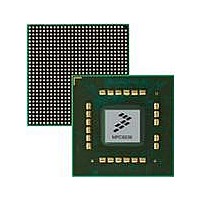
MPC8536DS Freescale Semiconductor, MPC8536DS Datasheet - Page 211

MPC8536DS
Manufacturer Part Number
MPC8536DS
Description
BOARD DEV SYSTEM MPC8536E
Manufacturer
Freescale Semiconductor
Series
PowerQUICC III™r
Type
MPUr
Datasheets
1.MPC8536EBVTAVLA.pdf
(127 pages)
2.MPC8536EBVTAVLA.pdf
(1706 pages)
3.MPC8536DS.pdf
(2 pages)
4.MPC8536DS.pdf
(126 pages)
Specifications of MPC8536DS
Contents
Board, Software and Documentation
Processor Series
MPC85xx
Core
e500
Data Bus Width
32 bit
Maximum Clock Frequency
667 MHz
Operating Supply Voltage
- 0.3 V to + 1.21 V
Maximum Operating Temperature
+ 105 C
Data Ram Size
32 KB
Interface Type
SPI, USB
Program Memory Type
DDR2, DDR3, SDRAM
Core Size
32 Bit
Program Memory Size
544KB
Cpu Speed
1.5GHz
Digital Ic Case Style
BGA
No. Of Pins
783
Supply Voltage Range
0.95V To 1.05V
Rohs Compliant
Yes
For Use With/related Products
MPC8536
Lead Free Status / RoHS Status
Lead free / RoHS Compliant
- MPC8536EBVTAVLA PDF datasheet
- MPC8536EBVTAVLA PDF datasheet #2
- MPC8536DS PDF datasheet #3
- MPC8536DS PDF datasheet #4
- Current page: 211 of 1706
- Download datasheet (15Mb)
16-bit addressable EEPROM memories are supported and detected automatically by the boot code. This
is accomplished by the boot code trying 16-bit mode if it fails to find the “BOOT” signature when in 24-bit
mode.
Figure 4-15
Output) modes of operation with a 24-bit addressable eSPI memory. With 16-bit addressable eSPI
memories, only a 16-bit address is transmitted, and valid data is received from the EEPROM on the 24th
SPI_CLK cycle rather than the 32nd SPI_CLK cycle for 24-bit addressable memories.
4.5.1.3
During boot from the on-chip ROM (for boot targets of either eSPI or SD/MMC), the user specifies 32-bit
addresses for several fields (Target Address for copying the user’s code, and the Execution Starting
Address). This section describes how these 32-bit effective addresses are translated into 36-bit real
addresses and the associated address translation and mapping.
The L2 cache remains disabled as per its power-on reset state. The e500 Level 1 and Level 2 MMU
configuration is left as per defaults, with the exception that the following TLB1 Entry 1 is also created (in
addition to the default TLB1 Entry 0 4kByte page at 0x0_FFFF_Fnnnn):
Freescale Semiconductor
•
•
•
•
•
•
•
SPI_MOSI
SPI_MISO
SPI_CLK
SPI_CS n
V=1 (valid)
TS=0 (address space 0)
TID=0x00 (global)
EPN[32–51]=0x00000
RPN[32–51]=0x00000
SIZE[0–3]=1011 (4 Gbyte)
SX/SR/SW=111 (Full supervisor mode access allowed)
shows the read instruction timing diagram for normal (not Atmel RapidS or Winbond Dual
Figure 4-15. Read Instruction Timing Diagram (24-bit addressable eSPI memory)
Default e500 Addressing During System Boot
MPC8536E PowerQUICC III Integrated Processor Reference Manual, Rev. 1
0
1
2
8-bit Instruction
3
0x03
4
High-Impedance
5
6
7
8
MSB
23 22 21
9
10 11
24-bit Address
Reset, Clocking, and Initialization
30 31 32 33 34 35
1
0
Data from EEPROM
MSB
4-41
Related parts for MPC8536DS
Image
Part Number
Description
Manufacturer
Datasheet
Request
R
Part Number:
Description:
Manufacturer:
Freescale Semiconductor, Inc
Datasheet:
Part Number:
Description:
Manufacturer:
Freescale Semiconductor, Inc
Datasheet:
Part Number:
Description:
Manufacturer:
Freescale Semiconductor, Inc
Datasheet:
Part Number:
Description:
Manufacturer:
Freescale Semiconductor, Inc
Datasheet:
Part Number:
Description:
Manufacturer:
Freescale Semiconductor, Inc
Datasheet:
Part Number:
Description:
Manufacturer:
Freescale Semiconductor, Inc
Datasheet:
Part Number:
Description:
Manufacturer:
Freescale Semiconductor, Inc
Datasheet:
Part Number:
Description:
Manufacturer:
Freescale Semiconductor, Inc
Datasheet:
Part Number:
Description:
Manufacturer:
Freescale Semiconductor, Inc
Datasheet:
Part Number:
Description:
Manufacturer:
Freescale Semiconductor, Inc
Datasheet:
Part Number:
Description:
Manufacturer:
Freescale Semiconductor, Inc
Datasheet:
Part Number:
Description:
Manufacturer:
Freescale Semiconductor, Inc
Datasheet:
Part Number:
Description:
Manufacturer:
Freescale Semiconductor, Inc
Datasheet:
Part Number:
Description:
Manufacturer:
Freescale Semiconductor, Inc
Datasheet:
Part Number:
Description:
Manufacturer:
Freescale Semiconductor, Inc
Datasheet:


