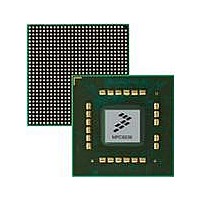
MPC8536DS Freescale Semiconductor, MPC8536DS Datasheet - Page 883

MPC8536DS
Manufacturer Part Number
MPC8536DS
Description
BOARD DEV SYSTEM MPC8536E
Manufacturer
Freescale Semiconductor
Series
PowerQUICC III™r
Type
MPUr
Datasheets
1.MPC8536EBVTAVLA.pdf
(127 pages)
2.MPC8536EBVTAVLA.pdf
(1706 pages)
3.MPC8536DS.pdf
(2 pages)
4.MPC8536DS.pdf
(126 pages)
Specifications of MPC8536DS
Contents
Board, Software and Documentation
Processor Series
MPC85xx
Core
e500
Data Bus Width
32 bit
Maximum Clock Frequency
667 MHz
Operating Supply Voltage
- 0.3 V to + 1.21 V
Maximum Operating Temperature
+ 105 C
Data Ram Size
32 KB
Interface Type
SPI, USB
Program Memory Type
DDR2, DDR3, SDRAM
Core Size
32 Bit
Program Memory Size
544KB
Cpu Speed
1.5GHz
Digital Ic Case Style
BGA
No. Of Pins
783
Supply Voltage Range
0.95V To 1.05V
Rohs Compliant
Yes
For Use With/related Products
MPC8536
Lead Free Status / RoHS Status
Lead free / RoHS Compliant
- MPC8536EBVTAVLA PDF datasheet
- MPC8536EBVTAVLA PDF datasheet #2
- MPC8536DS PDF datasheet #3
- MPC8536DS PDF datasheet #4
- Current page: 883 of 1706
- Download datasheet (15Mb)
14.5.4.2.2
Once synchronization is acquired, ordered_sets are decoded. If Configuration ordered_sets are received,
the eTSEC decodes the two octet data field and the sixteen-bit Configuration data is stored and used to
Auto-Negotiate with the link partner. in the Receive Configuration Register (RXCR[15:0]) an internal
register used to receive all the link partners informations and used to compare to local ability during
negotiation. Not visible to user. If, during Auto-Negotiation an invalid symbol is detected,
Auto-Negotiation re-starts. After Auto-Negotiation is completed the TBI MII Status Register SR[AN
done] in set. In this mode, packets may be received from the link partner.
14.5.4.3
This section describes the TBI MII registers. All of the TBI registers are 16 bits wide. The TBI registers
are accessed at the offset of the TBI physical address. The eTSEC’s TBI physical address is stored in the
TBIPA register. Writing to the TBI registers is performed in a way similar to writing to an external PHY,
using the MII management interface. Using TBIPA in place of the PHY address, in the MIIMADD[PHY
Address] field, and setting the MIIMADD[Register Address] to the appropriate address offset that
corresponds to the register that one wants to read or write (see
MIIMCOM[read cycle]) or write (writing to MIIMCON[PHY control]) to the TBI block. Refer to the TBI
physical address register in
MII register set in
registers and are only used for test and control of the eTSEC TBI block. The TBI’s TBI control register
(TBI) is for configuring the eTSEC ten-bit interface block. However, because this TBI block has an MII
management interface (just like any other PHY), it has an IEEE 802.3 register called the control register
(CR).
Freescale Semiconductor
1
0x02–0x03
R = Read-only, WO = Write Only, R/W = Read and Write, LH = Latches High, LL = Latches Low,
SC = Self-clearing,
Address
Offset
0x0F
0x00
0x01
0x04
0x05
0x06
0x07
0x08
0x10
0x11
TBI MII Set Register Descriptions
Auto-Negotiation for 1000BASE-X
Table
MPC8536E PowerQUICC III Integrated Processor Reference Manual, Rev. 1
Control (CR)
Status (SR)
Reserved
AN advertisement (ANA)
AN link partner base page ability
(ANLPBPA)
AN expansion (ANEX)
AN next page transmit (ANNPT)
AN link partner ability next page
(ANLPANP)
Extended status (EXST)
Jitter diagnostics (JD)
TBI control (TBICON)
14-130. Notice that jitter diagnostics and TBI control are not IEEE 802.3 required
TEN-BIT INTERFACE (TBI) REGISTERS
Section 14.5.3.1, “eTSEC General Control and Status
Table 14-130. TBI MII Register Set
Name
R, LH, LL
Access
R/W, R
RW, R
R, LH
R/W
R/W
R/W
R
R
R
R
Table
1
14-130), the user can read (set
Enhanced Three-Speed Ethernet Controllers
2 bytes
16 bits
16 bits
16 bits
16 bits
16 bits
16 bits
16 bits
16 bits
16 bits
16 bits
Size
14.5.4.3.10/14-145
14.5.4.3.1/14-136
14.5.4.3.2/14-137
14.5.4.3.2/14-137
14.5.4.3.4/14-140
14.5.4.3.5/14-141
14.5.4.3.6/14-141
14.5.4.3.7/14-142
14.5.4.3.8/14-143
14.5.4.3.9/14-144
Registers,” and the TBI
Section/page
14.5.4/14-133
—
14-135
Related parts for MPC8536DS
Image
Part Number
Description
Manufacturer
Datasheet
Request
R
Part Number:
Description:
Manufacturer:
Freescale Semiconductor, Inc
Datasheet:
Part Number:
Description:
Manufacturer:
Freescale Semiconductor, Inc
Datasheet:
Part Number:
Description:
Manufacturer:
Freescale Semiconductor, Inc
Datasheet:
Part Number:
Description:
Manufacturer:
Freescale Semiconductor, Inc
Datasheet:
Part Number:
Description:
Manufacturer:
Freescale Semiconductor, Inc
Datasheet:
Part Number:
Description:
Manufacturer:
Freescale Semiconductor, Inc
Datasheet:
Part Number:
Description:
Manufacturer:
Freescale Semiconductor, Inc
Datasheet:
Part Number:
Description:
Manufacturer:
Freescale Semiconductor, Inc
Datasheet:
Part Number:
Description:
Manufacturer:
Freescale Semiconductor, Inc
Datasheet:
Part Number:
Description:
Manufacturer:
Freescale Semiconductor, Inc
Datasheet:
Part Number:
Description:
Manufacturer:
Freescale Semiconductor, Inc
Datasheet:
Part Number:
Description:
Manufacturer:
Freescale Semiconductor, Inc
Datasheet:
Part Number:
Description:
Manufacturer:
Freescale Semiconductor, Inc
Datasheet:
Part Number:
Description:
Manufacturer:
Freescale Semiconductor, Inc
Datasheet:
Part Number:
Description:
Manufacturer:
Freescale Semiconductor, Inc
Datasheet:


