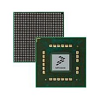
MPC8536DS Freescale Semiconductor, MPC8536DS Datasheet - Page 1210

MPC8536DS
Manufacturer Part Number
MPC8536DS
Description
BOARD DEV SYSTEM MPC8536E
Manufacturer
Freescale Semiconductor
Series
PowerQUICC III™r
Type
MPUr
Datasheets
1.MPC8536EBVTAVLA.pdf
(127 pages)
2.MPC8536EBVTAVLA.pdf
(1706 pages)
3.MPC8536DS.pdf
(2 pages)
4.MPC8536DS.pdf
(126 pages)
Specifications of MPC8536DS
Contents
Board, Software and Documentation
Processor Series
MPC85xx
Core
e500
Data Bus Width
32 bit
Maximum Clock Frequency
667 MHz
Operating Supply Voltage
- 0.3 V to + 1.21 V
Maximum Operating Temperature
+ 105 C
Data Ram Size
32 KB
Interface Type
SPI, USB
Program Memory Type
DDR2, DDR3, SDRAM
Core Size
32 Bit
Program Memory Size
544KB
Cpu Speed
1.5GHz
Digital Ic Case Style
BGA
No. Of Pins
783
Supply Voltage Range
0.95V To 1.05V
Rohs Compliant
Yes
For Use With/related Products
MPC8536
Lead Free Status / RoHS Status
Lead free / RoHS Compliant
- MPC8536EBVTAVLA PDF datasheet
- MPC8536EBVTAVLA PDF datasheet #2
- MPC8536DS PDF datasheet #3
- MPC8536DS PDF datasheet #4
- Current page: 1210 of 1706
- Download datasheet (15Mb)
PCI Express Interface Controller
allocates the appropriate data values to use. A write to the ATMU window containing the MSI address with
the appropriate data value generates the desired MSI transaction to the remote RC.
17.4.2.2
17.4.2.2.1
MSIs are the preferred interrupt signaling mechanism for PCI Express. However, in RC mode, the PCI
Express controller supports the INTx virtual-wire interrupt signaling mechanism (as described in the PCI
Express specification). Whenever the controller receives an inbound INTx (INTA, INTB, INTC, or INTD)
asserted or negated message, it asserts or negates an equivalent internal INTx signal (inta, intb, intc, or
intd) to the PIC.
The internal INTx signals from the PCI Express controller are logically combined with the interrupt
request (IRQn) input signals so that they share the same interrupt controlled by the associated EIVPRn and
EIDRn registers in the PIC. Refer to
information about handling of PCI Express INTx interrupts and the external interrupt request (IRQn)
signals.
If a PCI Express INTx interrupt is being used, then the PIC must be configured so that external interrupts
are active-low (EIVPRn[P] = 0), and level-sensitive (EIVPRn[S] = 1).
17.4.2.2.2
An inbound MSI cycle must hit into the PEXCSRBAR window with the address offset that points to the
MSIIR register in the PIC. Note that it is the responsibility of the host software to configure each EP’s MSI
capability registers such that an MSI cycle generated from the EP device is routed to the MSIIR register
in the PIC and for the appropriate interrupt to be generated to the core.
17.4.3
To prevent overflowing of the receiver’s buffers and for ordering compliance purposes, the transmitter
cannot send transactions unless it has enough flow control (FC) credits to send. Each device maintains an
FC credit pool. The FC information is conveyed between the two link partners by DLLPs during link
training (initial credit advertisement). The transaction layer performs the FC accounting functions. One FC
unit is four DWs (16-bytes) of data.
17-114
Initial Credit Advertisement
RC Handling of INTx Message and MSI Interrupts
INTx Message Handling
MSI Handling
NPH (Memory Read, IO Read, Cfg Read, Cfg Write)
MPC8536E PowerQUICC III Integrated Processor Reference Manual, Rev. 1
PH (Memory Write, Message Write)
PD (Memory Write, Message Write)
NPD (IO Write, Cfg Write)
Credit Type
Table 17-127. Initial credit advertisement
Chapter 9, “Programmable Interrupt Controller
Initial Credit Advertisement
(256/16)x4=64
4
8
2
Freescale Semiconductor
(PIC),” for more
Related parts for MPC8536DS
Image
Part Number
Description
Manufacturer
Datasheet
Request
R
Part Number:
Description:
Manufacturer:
Freescale Semiconductor, Inc
Datasheet:
Part Number:
Description:
Manufacturer:
Freescale Semiconductor, Inc
Datasheet:
Part Number:
Description:
Manufacturer:
Freescale Semiconductor, Inc
Datasheet:
Part Number:
Description:
Manufacturer:
Freescale Semiconductor, Inc
Datasheet:
Part Number:
Description:
Manufacturer:
Freescale Semiconductor, Inc
Datasheet:
Part Number:
Description:
Manufacturer:
Freescale Semiconductor, Inc
Datasheet:
Part Number:
Description:
Manufacturer:
Freescale Semiconductor, Inc
Datasheet:
Part Number:
Description:
Manufacturer:
Freescale Semiconductor, Inc
Datasheet:
Part Number:
Description:
Manufacturer:
Freescale Semiconductor, Inc
Datasheet:
Part Number:
Description:
Manufacturer:
Freescale Semiconductor, Inc
Datasheet:
Part Number:
Description:
Manufacturer:
Freescale Semiconductor, Inc
Datasheet:
Part Number:
Description:
Manufacturer:
Freescale Semiconductor, Inc
Datasheet:
Part Number:
Description:
Manufacturer:
Freescale Semiconductor, Inc
Datasheet:
Part Number:
Description:
Manufacturer:
Freescale Semiconductor, Inc
Datasheet:
Part Number:
Description:
Manufacturer:
Freescale Semiconductor, Inc
Datasheet:


