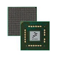
MPC8536DS Freescale Semiconductor, MPC8536DS Datasheet - Page 157

MPC8536DS
Manufacturer Part Number
MPC8536DS
Description
BOARD DEV SYSTEM MPC8536E
Manufacturer
Freescale Semiconductor
Series
PowerQUICC III™r
Type
MPUr
Datasheets
1.MPC8536EBVTAVLA.pdf
(127 pages)
2.MPC8536EBVTAVLA.pdf
(1706 pages)
3.MPC8536DS.pdf
(2 pages)
4.MPC8536DS.pdf
(126 pages)
Specifications of MPC8536DS
Contents
Board, Software and Documentation
Processor Series
MPC85xx
Core
e500
Data Bus Width
32 bit
Maximum Clock Frequency
667 MHz
Operating Supply Voltage
- 0.3 V to + 1.21 V
Maximum Operating Temperature
+ 105 C
Data Ram Size
32 KB
Interface Type
SPI, USB
Program Memory Type
DDR2, DDR3, SDRAM
Core Size
32 Bit
Program Memory Size
544KB
Cpu Speed
1.5GHz
Digital Ic Case Style
BGA
No. Of Pins
783
Supply Voltage Range
0.95V To 1.05V
Rohs Compliant
Yes
For Use With/related Products
MPC8536
Lead Free Status / RoHS Status
Lead free / RoHS Compliant
- MPC8536EBVTAVLA PDF datasheet
- MPC8536EBVTAVLA PDF datasheet #2
- MPC8536DS PDF datasheet #3
- MPC8536DS PDF datasheet #4
- Current page: 157 of 1706
- Download datasheet (15Mb)
USB1_PWRFAULT USB1 power fault
Freescale Semiconductor
TEMP_CATHODE
TEMP_ANODE
USB1_PCTL0
USB1_PCTL1
LSSD_MODE
CKSTP_OUT
MSRCID[2:4]
POWER_OK
USB1_D[7:0]
USB2_D[7:0]
POWER_EN
L1_TSTCLK
L2_TSTCLK
USB1_NXT
USB1_STP
USB1_CLK
TRIG_OUT
TEST_SEL
USB1_DIR
CLK_OUT
MSRCID0
MSRCID1
TRIG_IN
SYSCLK
ASLEEP
READY
MDVAL
Name
TRST
TDO
TMS
TCK
RTC
TDI
Table 3-1. MPC8536E Signal Reference by Functional Block (continued)
Checkstop out
Device ready
Asleep
Stable power
Power enable
Watchpoint trigger in
Watchpoint trigger out
Memory debug source port ID 0
Memory debug source port ID 1
Memory debug source port ID
2–4
Memory debug data valid
LSSD mode
L1 test clock
L2 test clock
Test select
Thermal diode access
Thermal diode access
Test clock
Test data in
Test data out
Test mode select
Test reset
System clock/PCI clock
Real time clock
Clock out
USB1 data
USB1 next data
USB1 data
USB1 stop
USB1 port control 0
USB1 port control 1
USB1 clock
USB2 data
MPC8536E PowerQUICC III Integrated Processor Reference Manual, Rev. 1
Description
System control
System control
Power mgmt
Power mgmt
Power mgmt
Functional
Debug
Debug
Debug
Debug
Debug
Debug
Block
USB1
USB1
USB1
USB1
USB1
USB1
USB1
USB1
USB2
Clock
Clock
Clock
JTAG
JTAG
JTAG
JTAG
JTAG
Test
Test
Test
Test
Test
Test
Alternate Function(s)
cfg_mem_debug
cfg_ddr_debug
TRIG_OUT
cfg_pci_clk
READY
GPIO6
GPIO7
—
—
—
—
—
—
—
—
—
—
—
—
—
—
—
—
—
—
—
—
—
—
—
—
—
—
—
Signals
No. of
1
1
1
1
1
1
1
1
1
3
1
1
1
1
1
2
2
1
1
1
1
1
1
1
1
8
1
1
1
1
1
1
1
8
I/O
I/O
I/O
O
O
O
O
O
O
O
O
O
O
O
O
O
O
I
I
I
I
I
I
I
I
I
I
I
I
I
I
I
I
I
I
Signal Descriptions
23-2/23-2
23-2/23-2
23-2/23-2
23-2/23-2
25-4/25-7
25-4/25-7
25-3/25-6
25-3/25-6
25-3/25-6
25-3/25-6
25-5/25-8
25-5/25-8
25-5/25-8
25-5/25-8
25-5/25-8
25-5/25-8
25-5/25-8
25-5/25-8
25-5/25-8
25-5/25-8
25-5/25-8
23-2/23-2
21-1/21-3
21-1/21-3
21-1/21-3
21-1/21-3
21-1/21-3
21-1/21-3
21-1/21-3
21-1/21-3
21-1/21-3
4-2/4-2
4-3/4-3
4-3/4-3
Table/
Page
3-7
Related parts for MPC8536DS
Image
Part Number
Description
Manufacturer
Datasheet
Request
R
Part Number:
Description:
Manufacturer:
Freescale Semiconductor, Inc
Datasheet:
Part Number:
Description:
Manufacturer:
Freescale Semiconductor, Inc
Datasheet:
Part Number:
Description:
Manufacturer:
Freescale Semiconductor, Inc
Datasheet:
Part Number:
Description:
Manufacturer:
Freescale Semiconductor, Inc
Datasheet:
Part Number:
Description:
Manufacturer:
Freescale Semiconductor, Inc
Datasheet:
Part Number:
Description:
Manufacturer:
Freescale Semiconductor, Inc
Datasheet:
Part Number:
Description:
Manufacturer:
Freescale Semiconductor, Inc
Datasheet:
Part Number:
Description:
Manufacturer:
Freescale Semiconductor, Inc
Datasheet:
Part Number:
Description:
Manufacturer:
Freescale Semiconductor, Inc
Datasheet:
Part Number:
Description:
Manufacturer:
Freescale Semiconductor, Inc
Datasheet:
Part Number:
Description:
Manufacturer:
Freescale Semiconductor, Inc
Datasheet:
Part Number:
Description:
Manufacturer:
Freescale Semiconductor, Inc
Datasheet:
Part Number:
Description:
Manufacturer:
Freescale Semiconductor, Inc
Datasheet:
Part Number:
Description:
Manufacturer:
Freescale Semiconductor, Inc
Datasheet:
Part Number:
Description:
Manufacturer:
Freescale Semiconductor, Inc
Datasheet:


