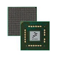
MPC8536DS Freescale Semiconductor, MPC8536DS Datasheet - Page 1104

MPC8536DS
Manufacturer Part Number
MPC8536DS
Description
BOARD DEV SYSTEM MPC8536E
Manufacturer
Freescale Semiconductor
Series
PowerQUICC III™r
Type
MPUr
Datasheets
1.MPC8536EBVTAVLA.pdf
(127 pages)
2.MPC8536EBVTAVLA.pdf
(1706 pages)
3.MPC8536DS.pdf
(2 pages)
4.MPC8536DS.pdf
(126 pages)
Specifications of MPC8536DS
Contents
Board, Software and Documentation
Processor Series
MPC85xx
Core
e500
Data Bus Width
32 bit
Maximum Clock Frequency
667 MHz
Operating Supply Voltage
- 0.3 V to + 1.21 V
Maximum Operating Temperature
+ 105 C
Data Ram Size
32 KB
Interface Type
SPI, USB
Program Memory Type
DDR2, DDR3, SDRAM
Core Size
32 Bit
Program Memory Size
544KB
Cpu Speed
1.5GHz
Digital Ic Case Style
BGA
No. Of Pins
783
Supply Voltage Range
0.95V To 1.05V
Rohs Compliant
Yes
For Use With/related Products
MPC8536
Lead Free Status / RoHS Status
Lead free / RoHS Compliant
- MPC8536EBVTAVLA PDF datasheet
- MPC8536EBVTAVLA PDF datasheet #2
- MPC8536DS PDF datasheet #3
- MPC8536DS PDF datasheet #4
- Current page: 1104 of 1706
- Download datasheet (15Mb)
PCI Express Interface Controller
17-8
0xDB4–
0xC54–
0xC74–
0xC94–
0xD14–
0xDBC
0xC5C
0xC6C
0xC7C
0xC8C
0xC9C
0xD9C
0xDAC
0xDB0
0xDC0
0xDC4
0xDC8
Offset
0xC60
0xC64
0xC68
0xC70
0xC80
0xC84
0xC88
0xC90
0xDA0
0xDA4
0xDA8
Reserved
PEXOTAR3—PCI Express outbound translation address register 3
PEXOTEAR3—PCI Express outbound translation extended address
register 3
PEXOWBAR3—PCI Express outbound window base address
register 3
Reserved
PEXOWAR3—PCI Express outbound window attributes register 3
Reserved
PEXOTAR4—PCI Express outbound translation address register 4
PEXOTEAR4—PCI Express outbound translation extended address
register 4
PEXOWBAR4—PCI Express outbound window base address
register 4
Reserved
PEXOWAR4—PCI Express outbound window attributes register 4
Reserved
Reserved
PEXITAR3—PCI Express inbound translation address register 3
Reserved
PEXIWBAR3—PCI Express inbound window base address register 3
PEXIWBEAR3—PCI Express inbound window base extended address
register 3
PEXIWAR3—PCI Express inbound window attributes register 3
Reserved
PEXITAR2—PCI Express inbound translation address register 2
Reserved
PEXIWBAR2—PCI Express inbound window base address register 2
Table 17-3. PCI Express Memory-Mapped Register Map (continued)
MPC8536E PowerQUICC III Integrated Processor Reference Manual, Rev. 1
PCI Express Controller 1 —Block Base Address 0x0_A000
PCI Express Controller 3—Block Base Address 0x0_B000
PCI Express Controller 2—Block Base Address 0x0_9000
Register
Outbound Window 3
Outbound Window 4
Inbound Window 3
Inbound Window 2
Access
R/W
R/W
R/W
R/W
R/W
R/W
R/W
R/W
R/W
R/W
R/W
R/W
R/W
R/W
—
—
—
—
—
—
—
—
—
0x0000_0000
0x0000_0000
0x0000_0000
0x0004_4023
0x0000_0000
0x0000_0000
0x0000_0000
0x0004_4023
0x0000_0000
0x0000_0000
0x0000_0000
0x20F4_4023
0x0000_0000
0x0000_0000
Reset
—
—
—
—
—
—
—
—
—
Freescale Semiconductor
17.3.5.1.1/17-20
17.3.5.1.2/17-21
17.3.5.1.3/17-22
17.3.5.1.4/17-22
17.3.5.1.1/17-20
17.3.5.1.2/17-21
17.3.5.1.3/17-22
17.3.5.1.4/17-22
17.3.5.2.3/17-26
17.3.5.2.4/17-27
17.3.5.2.5/17-27
17.3.5.2.6/17-28
17.3.5.2.3/17-26
17.3.5.2.4/17-27
Section/Page
Related parts for MPC8536DS
Image
Part Number
Description
Manufacturer
Datasheet
Request
R
Part Number:
Description:
Manufacturer:
Freescale Semiconductor, Inc
Datasheet:
Part Number:
Description:
Manufacturer:
Freescale Semiconductor, Inc
Datasheet:
Part Number:
Description:
Manufacturer:
Freescale Semiconductor, Inc
Datasheet:
Part Number:
Description:
Manufacturer:
Freescale Semiconductor, Inc
Datasheet:
Part Number:
Description:
Manufacturer:
Freescale Semiconductor, Inc
Datasheet:
Part Number:
Description:
Manufacturer:
Freescale Semiconductor, Inc
Datasheet:
Part Number:
Description:
Manufacturer:
Freescale Semiconductor, Inc
Datasheet:
Part Number:
Description:
Manufacturer:
Freescale Semiconductor, Inc
Datasheet:
Part Number:
Description:
Manufacturer:
Freescale Semiconductor, Inc
Datasheet:
Part Number:
Description:
Manufacturer:
Freescale Semiconductor, Inc
Datasheet:
Part Number:
Description:
Manufacturer:
Freescale Semiconductor, Inc
Datasheet:
Part Number:
Description:
Manufacturer:
Freescale Semiconductor, Inc
Datasheet:
Part Number:
Description:
Manufacturer:
Freescale Semiconductor, Inc
Datasheet:
Part Number:
Description:
Manufacturer:
Freescale Semiconductor, Inc
Datasheet:
Part Number:
Description:
Manufacturer:
Freescale Semiconductor, Inc
Datasheet:


