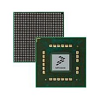
MPC8536DS Freescale Semiconductor, MPC8536DS Datasheet - Page 547

MPC8536DS
Manufacturer Part Number
MPC8536DS
Description
BOARD DEV SYSTEM MPC8536E
Manufacturer
Freescale Semiconductor
Series
PowerQUICC III™r
Type
MPUr
Datasheets
1.MPC8536EBVTAVLA.pdf
(127 pages)
2.MPC8536EBVTAVLA.pdf
(1706 pages)
3.MPC8536DS.pdf
(2 pages)
4.MPC8536DS.pdf
(126 pages)
Specifications of MPC8536DS
Contents
Board, Software and Documentation
Processor Series
MPC85xx
Core
e500
Data Bus Width
32 bit
Maximum Clock Frequency
667 MHz
Operating Supply Voltage
- 0.3 V to + 1.21 V
Maximum Operating Temperature
+ 105 C
Data Ram Size
32 KB
Interface Type
SPI, USB
Program Memory Type
DDR2, DDR3, SDRAM
Core Size
32 Bit
Program Memory Size
544KB
Cpu Speed
1.5GHz
Digital Ic Case Style
BGA
No. Of Pins
783
Supply Voltage Range
0.95V To 1.05V
Rohs Compliant
Yes
For Use With/related Products
MPC8536
Lead Free Status / RoHS Status
Lead free / RoHS Compliant
- MPC8536EBVTAVLA PDF datasheet
- MPC8536EBVTAVLA PDF datasheet #2
- MPC8536DS PDF datasheet #3
- MPC8536DS PDF datasheet #4
- Current page: 547 of 1706
- Download datasheet (15Mb)
Security Engine (SEC) 3.0
10.7.4.9
DEU IV Register
For CBC mode, the initialization vector is written to and read from the DEU IV register. The value of this
register changes as a result of the encryption process and reflects the context of DEU. Reading this memory
location while the module is processing data generates an error interrupt.
10.7.4.10 DEU Key Registers
The DEU uses three write-only key registers, K1, K2, and K3, to perform encryption and decryption. In
Single DES mode, only K1 may be written. The value written to K1 is simultaneously written to K3,
auto-enabling the DEU for 112-bit Triple DES if the key size register indicates 2 key 3DES is to be
performed (key size = 16 bytes). To operate in 168-bit Triple DES, K1 must be written first, followed by
the write of K2, then K3.
Reading any of these memory locations generates an address error interrupt.
10.7.4.11 DEU FIFOs
DEU uses an input FIFO/output FIFO pair to hold data before and after the encryption process. Normally,
the channels control all access to these FIFOs. For host-controlled operation, a write to anywhere in the
DEU FIFO address space enqueues data to the DEU input FIFO, and a read from anywhere in the DEU
FIFO address space dequeues data from the DEU output FIFO.
Writes to the input FIFO go first to a staging register which can be written by byte, word (4 bytes), or dword
(8 bytes). When all 8 bytes of the staging register have been written, the entire dword is automatically
enqueued into the FIFO. If any byte is written twice between enqueues, it causes an error interrupt of type
AE from the EU. Since the DEU data length should always be a multiple of 8 bytes, the last write should
complete a dword. However, if there is any partial dword in the staging register when the DEU end of
message register is written, the partial dword is automatically padded with zeros to a full 8 bytes and
enqueued to the input FIFO.
The output FIFO is readable by byte, word, or dword. When all 8 bytes of the head dword have been read,
that dword is automatically dequeued from the FIFO so that the next dword (if any) becomes available for
reading. If any byte is read twice between dequeues, it causes an error interrupt of type AE from the EU.
Overflows and underflows caused by reading or writing the DEU FIFOs are reflected in the DEU interrupt
status register.
10.7.5
Kasumi Execution Unit (KEU)
This section contains details about the Kasumi execution unit (KEU), including modes of operation, status
and control registers, and FIFOs. The KEU has been designed to support the f8 confidentiality function of
the 3GPP, GSM A5/3, EDGE A5/3, and GPRS GEA3 algorithms. The KEU also supports the 3GPP f9
integrity function.
Most of the registers described here would not normally be accessed by the host. They are documented
here mainly for debug purpose. In typical operation, the KEU is used through channel-controlled access,
which means that most reads and writes of the KEU registers are directed by the SEC channels. Driver
MPC8536E PowerQUICC III Integrated Processor Reference Manual, Rev. 1
Freescale Semiconductor
10-117
Related parts for MPC8536DS
Image
Part Number
Description
Manufacturer
Datasheet
Request
R
Part Number:
Description:
Manufacturer:
Freescale Semiconductor, Inc
Datasheet:
Part Number:
Description:
Manufacturer:
Freescale Semiconductor, Inc
Datasheet:
Part Number:
Description:
Manufacturer:
Freescale Semiconductor, Inc
Datasheet:
Part Number:
Description:
Manufacturer:
Freescale Semiconductor, Inc
Datasheet:
Part Number:
Description:
Manufacturer:
Freescale Semiconductor, Inc
Datasheet:
Part Number:
Description:
Manufacturer:
Freescale Semiconductor, Inc
Datasheet:
Part Number:
Description:
Manufacturer:
Freescale Semiconductor, Inc
Datasheet:
Part Number:
Description:
Manufacturer:
Freescale Semiconductor, Inc
Datasheet:
Part Number:
Description:
Manufacturer:
Freescale Semiconductor, Inc
Datasheet:
Part Number:
Description:
Manufacturer:
Freescale Semiconductor, Inc
Datasheet:
Part Number:
Description:
Manufacturer:
Freescale Semiconductor, Inc
Datasheet:
Part Number:
Description:
Manufacturer:
Freescale Semiconductor, Inc
Datasheet:
Part Number:
Description:
Manufacturer:
Freescale Semiconductor, Inc
Datasheet:
Part Number:
Description:
Manufacturer:
Freescale Semiconductor, Inc
Datasheet:
Part Number:
Description:
Manufacturer:
Freescale Semiconductor, Inc
Datasheet:


