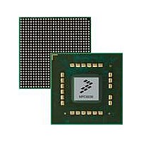
MPC8536DS Freescale Semiconductor, MPC8536DS Datasheet - Page 1590

MPC8536DS
Manufacturer Part Number
MPC8536DS
Description
BOARD DEV SYSTEM MPC8536E
Manufacturer
Freescale Semiconductor
Series
PowerQUICC III™r
Type
MPUr
Datasheets
1.MPC8536EBVTAVLA.pdf
(127 pages)
2.MPC8536EBVTAVLA.pdf
(1706 pages)
3.MPC8536DS.pdf
(2 pages)
4.MPC8536DS.pdf
(126 pages)
Specifications of MPC8536DS
Contents
Board, Software and Documentation
Processor Series
MPC85xx
Core
e500
Data Bus Width
32 bit
Maximum Clock Frequency
667 MHz
Operating Supply Voltage
- 0.3 V to + 1.21 V
Maximum Operating Temperature
+ 105 C
Data Ram Size
32 KB
Interface Type
SPI, USB
Program Memory Type
DDR2, DDR3, SDRAM
Core Size
32 Bit
Program Memory Size
544KB
Cpu Speed
1.5GHz
Digital Ic Case Style
BGA
No. Of Pins
783
Supply Voltage Range
0.95V To 1.05V
Rohs Compliant
Yes
For Use With/related Products
MPC8536
Lead Free Status / RoHS Status
Lead free / RoHS Compliant
- MPC8536EBVTAVLA PDF datasheet
- MPC8536EBVTAVLA PDF datasheet #2
- MPC8536DS PDF datasheet #3
- MPC8536DS PDF datasheet #4
- Current page: 1590 of 1706
- Download datasheet (15Mb)
Debug Features and Watchpoint Facility
25.2.2.3
Table 25-5
25-8
Signal
TDO
TMS
TCK
TDI
TRIG_OUT
Signal
shows detailed descriptions of the JTAG test signals.
Test Signals—Details
I/O
O JTAG test data output.
I
I
I
Table 25-4. Watchpoint and Trigger Signals—Detailed Signal Descriptions
Table 25-5. JTAG Test and Other Signals—Detailed Signal Descriptions
I/O
JTAG test clock.
JTAG test mode select.
O Trigger out. Function determined by TOSR[SEL]. When TOSR[SEL] is non-zero, it can be used
JTAG test data input.
Meaning
Meaning
Meaning
Meaning
MPC8536E PowerQUICC III Integrated Processor Reference Manual, Rev. 1
Timing
State
Timing See IEEE 1149.1 standard for more details.
Timing See IEEE 1149.1 standard for more details.
Timing See IEEE 1149.1 standard for more details.
for triggering external devices, like a logic analyzer, with either the watchpoint monitor, the trace
buffer, or the performance monitor as trigger sources. When TOSR[SEL] is cleared, TRIG_OUT
is multiplexed with READY, which indicates the operational readiness of the device (running or in
low-power or debug modes). See
“Global Utilities,”
Meaning
State
State
State
Timing Assertion may occur at any time. Remains asserted for at least 3 system clocks
State
Asserted/Negated—Should be driven by a free-running clock signal with a 30–70% duty cycle.
Asserted/Negated—The value present on the rising edge of TCK is clocked into the selected
See IEEE 1149.1 standard for more details.
Asserted/Negated—The contents of the selected internal instruction or data register are
Asserted/Negated—Decoded by the internal JTAG TAP controller to distinguish the primary
Asserted—When TOSR[SEL] is all zeros, serves as the READY signal, indicating that
Negation—No final watchpoint match condition
Input signals to the TAP are clocked in on the rising edge. Changes to the TAP output
signals occur on the falling edge. The test logic allows TCK to be stopped. An
unterminated input appears as a high signal level to the test logic due to an internal
pull-up resistor.
JTAG test instruction or data register. An unterminated input appears as a high signal
level to the test logic due to an internal pull-up resistor.
shifted out on this signal on the falling edge of TCK. Remains in a high-impedance state
except when scanning data.
operation of the test support circuitry. An unterminated input appears as a high signal
level to the test logic due to an internal pull-up resistor.
the device is not in a low-power or debug mode and that it has emerged from
reset. SEL
for more details about reset, low-power, and debug states.
0 indicates that a programmed trigger event has occurred.
Chapter 4, “Reset, Clocking, and Initialization,”
Description
Description
Freescale Semiconductor
and
Chapter 23,
Related parts for MPC8536DS
Image
Part Number
Description
Manufacturer
Datasheet
Request
R
Part Number:
Description:
Manufacturer:
Freescale Semiconductor, Inc
Datasheet:
Part Number:
Description:
Manufacturer:
Freescale Semiconductor, Inc
Datasheet:
Part Number:
Description:
Manufacturer:
Freescale Semiconductor, Inc
Datasheet:
Part Number:
Description:
Manufacturer:
Freescale Semiconductor, Inc
Datasheet:
Part Number:
Description:
Manufacturer:
Freescale Semiconductor, Inc
Datasheet:
Part Number:
Description:
Manufacturer:
Freescale Semiconductor, Inc
Datasheet:
Part Number:
Description:
Manufacturer:
Freescale Semiconductor, Inc
Datasheet:
Part Number:
Description:
Manufacturer:
Freescale Semiconductor, Inc
Datasheet:
Part Number:
Description:
Manufacturer:
Freescale Semiconductor, Inc
Datasheet:
Part Number:
Description:
Manufacturer:
Freescale Semiconductor, Inc
Datasheet:
Part Number:
Description:
Manufacturer:
Freescale Semiconductor, Inc
Datasheet:
Part Number:
Description:
Manufacturer:
Freescale Semiconductor, Inc
Datasheet:
Part Number:
Description:
Manufacturer:
Freescale Semiconductor, Inc
Datasheet:
Part Number:
Description:
Manufacturer:
Freescale Semiconductor, Inc
Datasheet:
Part Number:
Description:
Manufacturer:
Freescale Semiconductor, Inc
Datasheet:


