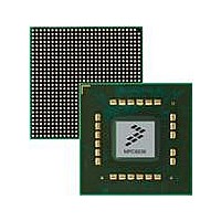
MPC8536DS Freescale Semiconductor, MPC8536DS Datasheet - Page 1226

MPC8536DS
Manufacturer Part Number
MPC8536DS
Description
BOARD DEV SYSTEM MPC8536E
Manufacturer
Freescale Semiconductor
Series
PowerQUICC III™r
Type
MPUr
Datasheets
1.MPC8536EBVTAVLA.pdf
(127 pages)
2.MPC8536EBVTAVLA.pdf
(1706 pages)
3.MPC8536DS.pdf
(2 pages)
4.MPC8536DS.pdf
(126 pages)
Specifications of MPC8536DS
Contents
Board, Software and Documentation
Processor Series
MPC85xx
Core
e500
Data Bus Width
32 bit
Maximum Clock Frequency
667 MHz
Operating Supply Voltage
- 0.3 V to + 1.21 V
Maximum Operating Temperature
+ 105 C
Data Ram Size
32 KB
Interface Type
SPI, USB
Program Memory Type
DDR2, DDR3, SDRAM
Core Size
32 Bit
Program Memory Size
544KB
Cpu Speed
1.5GHz
Digital Ic Case Style
BGA
No. Of Pins
783
Supply Voltage Range
0.95V To 1.05V
Rohs Compliant
Yes
For Use With/related Products
MPC8536
Lead Free Status / RoHS Status
Lead free / RoHS Compliant
- MPC8536EBVTAVLA PDF datasheet
- MPC8536EBVTAVLA PDF datasheet #2
- MPC8536DS PDF datasheet #3
- MPC8536DS PDF datasheet #4
- Current page: 1226 of 1706
- Download datasheet (15Mb)
Enhanced Serial Peripheral Interface
18.3.1.7
The eSPI CSn mode registers (SPMODEn), shown in
chip select n.
Table 18-8
18-12
Offset SPMODE0: 0x020
Reset
Reset
9–10
Bits
4–7
W
W
R
R
0
1
2
3
8
SPMODE1: 0x024
SPMODE2: 0x028
SPMODE3: 0x02C
CI n
16
0
0
DIV16 n Divide by 16. Selects the clock source for the eSPI baud rate generator(eSPI BRG) when configured
Name
ODD n
REV n
describes the SPMODEn fields.
PM n
CP n
CI n
—
eSPI CS n Mode Registers (SPMODE0–4)
CP n REV n DIV16 n
17
0
1
CS n BEF
Clock invert. Inverts eSPI clock polarity. See
0 The inactive state of SPI_CLK is low.
1 The inactive state of SPI_CLK is high.
Clock phase. Selects the transfer format. See
0 SPI_CLK starts toggling at the middle of the data transfer.
1 SPI_CLK starts toggling at the beginning of the data transfer.
Reverse data mode. Determines the receive and transmit character bit order.
0 lsb of the character sent and received first
1 msb of the character sent and received first - for 8/16 bits data character only
0 System clock is the input to the eSPI BRG.
1 System clock/16 is the input to the eSPI BRG.
Note: System clock is defined to be CCB clock divided by 2
Prescale modulus select. Specifies the divide ratio of the prescale divider in the eSPI clock generator.
Note: System clock is defined to be CCB clock divided by 2
0 Even division: 2*(PM+1)*(15*DIV16+1); 50% duty cycle
1 Odd division: (2*PM + 1)*(15*DIV16+1) (except for PM=0 where it divides by 2*(7*DIV16+1)); duty
Reserved, should be cleared.
MPC8536E PowerQUICC III Integrated Processor Reference Manual, Rev. 1
as an eSPI master.
The eSPI baud rate generator clock source (either system clock or system clock divided by 16,
depending on DIV16 bit) is divided by 2* ([PM] + 1), a range from 2 to 32. For example, if the prescale
modulus is set to PM=0x0011 and DIV16 is set, the SPI_CLK/system clock rate will be
16*(2*(0x0011+1))=128
cycle is (PM+1)/(2*PM+1) for DIV16=0; duty cycle is 50% for DIV16=1
18
0
2
Figure 18-17. eSPI CS n Mode Register (SPMODE n )
19
0
3
Table 18-8. SPMODE n Field Descriptions
20
0
4
CS n AFT
0
PM n
0
All zeros
23
Figure
0
7
Description
Figure 18-18
Figure 18-18
ODD n
24
0
8
18-17, control eSPI master operation with
and
and
0
9
Figure 18-19
—
CS n CG
Figure 18-19
10
0
POL n
11
1
for more information
for more information.
Freescale Semiconductor
12
28
0
Access: Read/Write
29
0
LEN n
0
—
15
31
0
Related parts for MPC8536DS
Image
Part Number
Description
Manufacturer
Datasheet
Request
R
Part Number:
Description:
Manufacturer:
Freescale Semiconductor, Inc
Datasheet:
Part Number:
Description:
Manufacturer:
Freescale Semiconductor, Inc
Datasheet:
Part Number:
Description:
Manufacturer:
Freescale Semiconductor, Inc
Datasheet:
Part Number:
Description:
Manufacturer:
Freescale Semiconductor, Inc
Datasheet:
Part Number:
Description:
Manufacturer:
Freescale Semiconductor, Inc
Datasheet:
Part Number:
Description:
Manufacturer:
Freescale Semiconductor, Inc
Datasheet:
Part Number:
Description:
Manufacturer:
Freescale Semiconductor, Inc
Datasheet:
Part Number:
Description:
Manufacturer:
Freescale Semiconductor, Inc
Datasheet:
Part Number:
Description:
Manufacturer:
Freescale Semiconductor, Inc
Datasheet:
Part Number:
Description:
Manufacturer:
Freescale Semiconductor, Inc
Datasheet:
Part Number:
Description:
Manufacturer:
Freescale Semiconductor, Inc
Datasheet:
Part Number:
Description:
Manufacturer:
Freescale Semiconductor, Inc
Datasheet:
Part Number:
Description:
Manufacturer:
Freescale Semiconductor, Inc
Datasheet:
Part Number:
Description:
Manufacturer:
Freescale Semiconductor, Inc
Datasheet:
Part Number:
Description:
Manufacturer:
Freescale Semiconductor, Inc
Datasheet:


