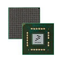
MPC8536DS Freescale Semiconductor, MPC8536DS Datasheet - Page 654

MPC8536DS
Manufacturer Part Number
MPC8536DS
Description
BOARD DEV SYSTEM MPC8536E
Manufacturer
Freescale Semiconductor
Series
PowerQUICC III™r
Type
MPUr
Datasheets
1.MPC8536EBVTAVLA.pdf
(127 pages)
2.MPC8536EBVTAVLA.pdf
(1706 pages)
3.MPC8536DS.pdf
(2 pages)
4.MPC8536DS.pdf
(126 pages)
Specifications of MPC8536DS
Contents
Board, Software and Documentation
Processor Series
MPC85xx
Core
e500
Data Bus Width
32 bit
Maximum Clock Frequency
667 MHz
Operating Supply Voltage
- 0.3 V to + 1.21 V
Maximum Operating Temperature
+ 105 C
Data Ram Size
32 KB
Interface Type
SPI, USB
Program Memory Type
DDR2, DDR3, SDRAM
Core Size
32 Bit
Program Memory Size
544KB
Cpu Speed
1.5GHz
Digital Ic Case Style
BGA
No. Of Pins
783
Supply Voltage Range
0.95V To 1.05V
Rohs Compliant
Yes
For Use With/related Products
MPC8536
Lead Free Status / RoHS Status
Lead free / RoHS Compliant
- MPC8536EBVTAVLA PDF datasheet
- MPC8536EBVTAVLA PDF datasheet #2
- MPC8536DS PDF datasheet #3
- MPC8536DS PDF datasheet #4
- Current page: 654 of 1706
- Download datasheet (15Mb)
Enhanced Local Bus Controller
13.3.1.2
The ORn registers define the sizes of memory banks and access attributes. The ORn attribute bits support
the following three modes of operation as defined by BRn[MSEL]:
13-12
21–22
24–26
28–29
Bits
23
27
30
31
•
•
•
GPCM mode
FCM mode
UPM mode
DECC Specifies the method for data error checking.
Name
MSEL Machine select. Specifies the machine to use for handling memory operations.
ATOM Atomic operation. Writes (reads) to the address space handled by the memory controller bank reserve the
WP
—
—
V
Option Registers (OR0–OR7)
00 Data error checking disabled, but normal parity generation for GPCM and UPM. No ECC generation for
01 Normal parity generation and checking for GPCM and UPM. ECC checking is enabled, but ECC
10 Read-modify-write parity generation and normal parity checking for GPCM and UPM. ECC checking and
11 Reserved
Write protect.
0 Read and write accesses are allowed.
1 Only read accesses are allowed. The memory controller does not assert LCS n on write cycles to this
000 GPCM (possible reset value)
001 FCM (possible reset value)
010 Reserved
011 Reserved
100 UPMA
101 UPMB
110 UPMC
111 Reserved
Reserved
selected memory bank for the exclusive use of the accessing device. The reservation is released when the
device performs a read (write) operation to this memory controller bank. If a subsequent read (write) request
to this memory controller bank is not detected within 256 bus clock cycles of the last write (read), the
reservation is released and an atomic error is reported (if enabled).
00 The address space controlled by this bank is not used for atomic operations.
01 Read-after-write-atomic (RAWA).
10 Write-after-read-atomic (WARA).
11 Reserved
Reserved
Valid bit. Indicates that the contents of the BR n and OR n pair are valid. LCS n does not assert unless V is set
(an access to a region that has no valid bit set may cause a bus time-out). After a system reset, only BR0[V]
is set.
0 This bank is invalid.
1 This bank is valid.
memory bank. LTESR[WP] is set (if WP is set) if a write to this memory bank is attempted, and a local bus
error interrupt is generated (if enabled), terminating the cycle.
FCM.
generation is disabled, for FCM on full-page transfers.
generation are enabled for FCM on full-page transfers.
MPC8536E PowerQUICC III Integrated Processor Reference Manual, Rev. 1
Table 13-4. BR n Field Descriptions (continued)
Description
Freescale Semiconductor
Related parts for MPC8536DS
Image
Part Number
Description
Manufacturer
Datasheet
Request
R
Part Number:
Description:
Manufacturer:
Freescale Semiconductor, Inc
Datasheet:
Part Number:
Description:
Manufacturer:
Freescale Semiconductor, Inc
Datasheet:
Part Number:
Description:
Manufacturer:
Freescale Semiconductor, Inc
Datasheet:
Part Number:
Description:
Manufacturer:
Freescale Semiconductor, Inc
Datasheet:
Part Number:
Description:
Manufacturer:
Freescale Semiconductor, Inc
Datasheet:
Part Number:
Description:
Manufacturer:
Freescale Semiconductor, Inc
Datasheet:
Part Number:
Description:
Manufacturer:
Freescale Semiconductor, Inc
Datasheet:
Part Number:
Description:
Manufacturer:
Freescale Semiconductor, Inc
Datasheet:
Part Number:
Description:
Manufacturer:
Freescale Semiconductor, Inc
Datasheet:
Part Number:
Description:
Manufacturer:
Freescale Semiconductor, Inc
Datasheet:
Part Number:
Description:
Manufacturer:
Freescale Semiconductor, Inc
Datasheet:
Part Number:
Description:
Manufacturer:
Freescale Semiconductor, Inc
Datasheet:
Part Number:
Description:
Manufacturer:
Freescale Semiconductor, Inc
Datasheet:
Part Number:
Description:
Manufacturer:
Freescale Semiconductor, Inc
Datasheet:
Part Number:
Description:
Manufacturer:
Freescale Semiconductor, Inc
Datasheet:


