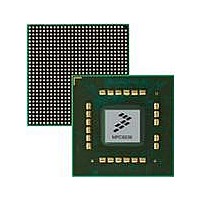
MPC8536DS Freescale Semiconductor, MPC8536DS Datasheet - Page 673

MPC8536DS
Manufacturer Part Number
MPC8536DS
Description
BOARD DEV SYSTEM MPC8536E
Manufacturer
Freescale Semiconductor
Series
PowerQUICC III™r
Type
MPUr
Datasheets
1.MPC8536EBVTAVLA.pdf
(127 pages)
2.MPC8536EBVTAVLA.pdf
(1706 pages)
3.MPC8536DS.pdf
(2 pages)
4.MPC8536DS.pdf
(126 pages)
Specifications of MPC8536DS
Contents
Board, Software and Documentation
Processor Series
MPC85xx
Core
e500
Data Bus Width
32 bit
Maximum Clock Frequency
667 MHz
Operating Supply Voltage
- 0.3 V to + 1.21 V
Maximum Operating Temperature
+ 105 C
Data Ram Size
32 KB
Interface Type
SPI, USB
Program Memory Type
DDR2, DDR3, SDRAM
Core Size
32 Bit
Program Memory Size
544KB
Cpu Speed
1.5GHz
Digital Ic Case Style
BGA
No. Of Pins
783
Supply Voltage Range
0.95V To 1.05V
Rohs Compliant
Yes
For Use With/related Products
MPC8536
Lead Free Status / RoHS Status
Lead free / RoHS Compliant
- MPC8536EBVTAVLA PDF datasheet
- MPC8536EBVTAVLA PDF datasheet #2
- MPC8536DS PDF datasheet #3
- MPC8536DS PDF datasheet #4
- Current page: 673 of 1706
- Download datasheet (15Mb)
Table 13-19
13.3.1.13 Transfer Error Address Register (LTEAR)
The transfer error address register (LTEAR) captures the address of a transaction that caused an
error/event. The transfer error address register (LTEAR) is shown in
Table 13-20
13.3.1.14 Transfer Error ECC Register (LTECCR)
The transfer error ECC register (LTECCR) captures single bit and multibit errors per 512-byte sector in
FCM mode. LTECCR, shown in
Freescale Semiconductor
11–15
16–19
20–27
28–30
4–10
Offset 0x0_50C0
0–31
Reset
Bits
Bits
0–2
31
3
W
R
0
SRCID Captures the source of the transaction when this information is provided on the internal interface to the eLBC.
Name
Name
RWB
BNK
PB
—
—
—
V
A
describes LTEATR fields.
describes LTEAR fields.
Reserved
Transaction type for the error:
0 The transaction for the error was a write transaction.
1 The transaction for the error was a read transaction.
Reserved
Parity error on byte or block. For GPCM and UPM, there are four parity error status bits, one per byte lane. A
bit is set for the byte that had a parity error (bit 16 represents byte 0, the most significant byte lane). For FCM,
there are at most four 512-byte page blocks (for a large page device) checked by ECC. A bit is set for the
512-byte block that had an uncorrectable ECC error on read (bit 16 represents block 0, the first 512 bytes of
a page; if ORx[PGS] = 0, bits 17–19 are always 0).
Memory controller bank. There is one error status bit per memory controller bank (bit 20 represents bank 0).
A bit is set for the local bus memory controller bank that had an error.
Reserved
Error attribute capture is valid. Indicates that the captured error information is valid.
0 Captured error attributes and address are not valid.
1 Captured error attributes and address are valid.
Transaction address for the error. For GPCM and UPM, holds the 32-bit address of the transaction resulting
in an error. For FCM, this register is undefined.
MPC8536E PowerQUICC III Integrated Processor Reference Manual, Rev. 1
Figure 13-17. Transfer Error Address Register (LTEAR)
Figure
Table 13-19. LTEATR Field Descriptions
Table 13-20. LTEAR Field Descriptions
13-18, is a write-1-to-clear register. Write operations can clear but
All zeros
Description
Description
A
Figure
13-17.
Enhanced Local Bus Controller
Access: Read/Write
13-31
31
Related parts for MPC8536DS
Image
Part Number
Description
Manufacturer
Datasheet
Request
R
Part Number:
Description:
Manufacturer:
Freescale Semiconductor, Inc
Datasheet:
Part Number:
Description:
Manufacturer:
Freescale Semiconductor, Inc
Datasheet:
Part Number:
Description:
Manufacturer:
Freescale Semiconductor, Inc
Datasheet:
Part Number:
Description:
Manufacturer:
Freescale Semiconductor, Inc
Datasheet:
Part Number:
Description:
Manufacturer:
Freescale Semiconductor, Inc
Datasheet:
Part Number:
Description:
Manufacturer:
Freescale Semiconductor, Inc
Datasheet:
Part Number:
Description:
Manufacturer:
Freescale Semiconductor, Inc
Datasheet:
Part Number:
Description:
Manufacturer:
Freescale Semiconductor, Inc
Datasheet:
Part Number:
Description:
Manufacturer:
Freescale Semiconductor, Inc
Datasheet:
Part Number:
Description:
Manufacturer:
Freescale Semiconductor, Inc
Datasheet:
Part Number:
Description:
Manufacturer:
Freescale Semiconductor, Inc
Datasheet:
Part Number:
Description:
Manufacturer:
Freescale Semiconductor, Inc
Datasheet:
Part Number:
Description:
Manufacturer:
Freescale Semiconductor, Inc
Datasheet:
Part Number:
Description:
Manufacturer:
Freescale Semiconductor, Inc
Datasheet:
Part Number:
Description:
Manufacturer:
Freescale Semiconductor, Inc
Datasheet:


