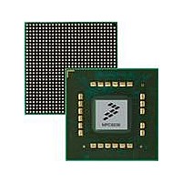
MPC8536DS Freescale Semiconductor, MPC8536DS Datasheet - Page 755

MPC8536DS
Manufacturer Part Number
MPC8536DS
Description
BOARD DEV SYSTEM MPC8536E
Manufacturer
Freescale Semiconductor
Series
PowerQUICC III™r
Type
MPUr
Datasheets
1.MPC8536EBVTAVLA.pdf
(127 pages)
2.MPC8536EBVTAVLA.pdf
(1706 pages)
3.MPC8536DS.pdf
(2 pages)
4.MPC8536DS.pdf
(126 pages)
Specifications of MPC8536DS
Contents
Board, Software and Documentation
Processor Series
MPC85xx
Core
e500
Data Bus Width
32 bit
Maximum Clock Frequency
667 MHz
Operating Supply Voltage
- 0.3 V to + 1.21 V
Maximum Operating Temperature
+ 105 C
Data Ram Size
32 KB
Interface Type
SPI, USB
Program Memory Type
DDR2, DDR3, SDRAM
Core Size
32 Bit
Program Memory Size
544KB
Cpu Speed
1.5GHz
Digital Ic Case Style
BGA
No. Of Pins
783
Supply Voltage Range
0.95V To 1.05V
Rohs Compliant
Yes
For Use With/related Products
MPC8536
Lead Free Status / RoHS Status
Lead free / RoHS Compliant
- MPC8536EBVTAVLA PDF datasheet
- MPC8536EBVTAVLA PDF datasheet #2
- MPC8536DS PDF datasheet #3
- MPC8536DS PDF datasheet #4
- Current page: 755 of 1706
- Download datasheet (15Mb)
Table 14-1
Freescale Semiconductor
TSEC n _GTX_CLK
EC_GTX_CLK125
TSEC n _RXD[7:4]
TSEC n _RXD[3:0]
TSEC n _RX_CLK
TSEC n _RX_DV
•
•
•
•
•
Signal Name
TSEC n _COL
TSEC n _CRS
EC_MDIO
EC_MDC
The TBI interface shares signals with the GMII interface signals.
The RGMII, RTBI, and RMII options are reduced-pin implementations of the GMII, TBI, and MII
interfaces, respectively.
SGMII interfaces are offered via the SerDes interface signals.
1588 timer signals
Finally, the FIFO interfaces share the GMII signals—8 bits of data plus 3 bits of control signals.
lists the network interface signals.
MPC8536E PowerQUICC III Integrated Processor Reference Manual, Rev. 1
MII—collision, input
FIFO—transmit flow control, input
MII—carrier sense, input
TBI—signal detect, input
FIFO—receive flow control, output
RTBI, RGMII—inverted transmit clock feedback, output
TBIFIFO—continuous transmit clock feedback, output
GMII, MII, RMII—transmit clock feedback when transmission is enabled, zero otherwise,
output
Oscillator source for GMII, TBI, RGMII, RTBI transmit clock, input, shared by all eTSECs
Management clock, output.
Management data, bidirectional.
GMII, MII, RGMII—receive clock, input
TBI—PMA receive clock 0, input
FIFO—receive clock, input
GMII, MII—receive data valid, input
TBI—receive code group (RCG) bit 8, input
RGMII (RX_CLK rising)—receive data valid, input
RGMII (RX_CLK falling)—receive error, input
RTBI (RX_CLK rising)—receive code group (RCG) bit 4, input
RTBI (RX_CLK falling)—receive code group (RCG) bit 9, input
RMII—CRS_DV carrier sense/data valid, input
FIFO—receive data valid or receive control bit, input
GMII—receive data bits 7:4 input
TBI—RCG bits 7:4, input
FIFO—receive data bits 7:4 input
MII, RGMII, RTBI, RMII—unused
GMII, MII—Receive data bits 3:0, input
TBI—RGC bits 3:0, input
RGMII (RX_CLK rising) —Receive data bits 3:0, input
RGMII (RX_CLK falling)—Receive data bits 7:4, input
RTBI (RX_CLK rising)—RCG bits 3:0, input
RTBI (RX_CLK falling)—RCG bits 8:5, input
RMII—RXD[1:0] receive data bits, input
RMII—RXD[3:2] are unused
FIFO—Receive data bits 3:0, input
Table 14-1. eTSEC n Network Interface Signal Properties
Function
Enhanced Three-Speed Ethernet Controllers
Hi-Z (input)
Reset
State
—
—
—
—
—
—
—
0
0
14-7
Related parts for MPC8536DS
Image
Part Number
Description
Manufacturer
Datasheet
Request
R
Part Number:
Description:
Manufacturer:
Freescale Semiconductor, Inc
Datasheet:
Part Number:
Description:
Manufacturer:
Freescale Semiconductor, Inc
Datasheet:
Part Number:
Description:
Manufacturer:
Freescale Semiconductor, Inc
Datasheet:
Part Number:
Description:
Manufacturer:
Freescale Semiconductor, Inc
Datasheet:
Part Number:
Description:
Manufacturer:
Freescale Semiconductor, Inc
Datasheet:
Part Number:
Description:
Manufacturer:
Freescale Semiconductor, Inc
Datasheet:
Part Number:
Description:
Manufacturer:
Freescale Semiconductor, Inc
Datasheet:
Part Number:
Description:
Manufacturer:
Freescale Semiconductor, Inc
Datasheet:
Part Number:
Description:
Manufacturer:
Freescale Semiconductor, Inc
Datasheet:
Part Number:
Description:
Manufacturer:
Freescale Semiconductor, Inc
Datasheet:
Part Number:
Description:
Manufacturer:
Freescale Semiconductor, Inc
Datasheet:
Part Number:
Description:
Manufacturer:
Freescale Semiconductor, Inc
Datasheet:
Part Number:
Description:
Manufacturer:
Freescale Semiconductor, Inc
Datasheet:
Part Number:
Description:
Manufacturer:
Freescale Semiconductor, Inc
Datasheet:
Part Number:
Description:
Manufacturer:
Freescale Semiconductor, Inc
Datasheet:


