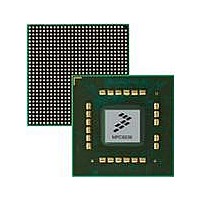
MPC8536DS Freescale Semiconductor, MPC8536DS Datasheet - Page 622

MPC8536DS
Manufacturer Part Number
MPC8536DS
Description
BOARD DEV SYSTEM MPC8536E
Manufacturer
Freescale Semiconductor
Series
PowerQUICC III™r
Type
MPUr
Datasheets
1.MPC8536EBVTAVLA.pdf
(127 pages)
2.MPC8536EBVTAVLA.pdf
(1706 pages)
3.MPC8536DS.pdf
(2 pages)
4.MPC8536DS.pdf
(126 pages)
Specifications of MPC8536DS
Contents
Board, Software and Documentation
Processor Series
MPC85xx
Core
e500
Data Bus Width
32 bit
Maximum Clock Frequency
667 MHz
Operating Supply Voltage
- 0.3 V to + 1.21 V
Maximum Operating Temperature
+ 105 C
Data Ram Size
32 KB
Interface Type
SPI, USB
Program Memory Type
DDR2, DDR3, SDRAM
Core Size
32 Bit
Program Memory Size
544KB
Cpu Speed
1.5GHz
Digital Ic Case Style
BGA
No. Of Pins
783
Supply Voltage Range
0.95V To 1.05V
Rohs Compliant
Yes
For Use With/related Products
MPC8536
Lead Free Status / RoHS Status
Lead free / RoHS Compliant
- MPC8536EBVTAVLA PDF datasheet
- MPC8536EBVTAVLA PDF datasheet #2
- MPC8536DS PDF datasheet #3
- MPC8536DS PDF datasheet #4
- Current page: 622 of 1706
- Download datasheet (15Mb)
DUART
the alternate function register. Refer to
information on ULCR[DLAB].
All the DUART registers are one byte wide. Reads and writes to these registers must be byte-wide
operations.
detailed information about each register. Undefined byte address spaces within offset 0x000–0xFFF are
reserved.
In this table and in the register figures and field descriptions, the following access definitions apply:
12-4
1
•
•
•
•
•
UART1 has the same memory-mapped registers that are described for UART0 from 0x500 to 0x510, except the offsets
range from 0x600 to 0x610.
0x600–
0x500
0x500
0x500
0x501
0x501
0x502
0x502
0x502
0x503
0x504
0x505
0x506
0x507
0x510
0x610
Offset
Reserved fields are always ignored for the purposes of determining access type.
R/W, R, and W (read/write, read only, and write only) indicate that all the non-reserved fields in a
register have the same access type.
w1c indicates that all of the non-reserved fields in a register are cleared by writing ones to them.
Mixed indicates a combination of access types.
Special is used when no other category applies. In this case the register figure and field description
table should be read carefully.
Table 12-2
URBR—ULCR[DLAB] = 0 UART0 receiver buffer register
UTHR—ULCR[DLAB] = 0 UART0 transmitter holding register
UDLB—ULCR[DLAB] = 1 UART0 divisor least significant byte register
UIER—ULCR[DLAB] = 0 UART0 interrupt enable register
UDMB—ULCR[DLAB] = 1 UART0 divisor most significant byte register
UIIR—ULCR[DLAB] = 0 UART0 interrupt ID register
UFCR—ULCR[DLAB] = 0 UART0 FIFO control register
UAFR—ULCR[DLAB] = 1 UART0 alternate function register
ULCR—ULCR[DLAB] = x UART0 line control register
UMCR—ULCR[DLAB] = x UART0 modem control register
ULSR—ULCR[DLAB] = x UART0 line status register
UMSR—ULCR[DLAB] = x UART0 modem status register
USCR—ULCR[DLAB] = x UART0 scratch register
UDSR—ULCR[DLAB] = x UART0 DMA status register
UART1 Registers
MPC8536E PowerQUICC III Integrated Processor Reference Manual, Rev. 1
provides a register summary with references to the section and page that contains
1
Table 12-2. DUART Register Summary
DUART—Block Base Address 0x0_4000
Section 12.3.1.8, “Line Control Registers (ULCRn),”
Register
UART0 Registers
UART1 Registers
Access Reset
R/W
R/W
R/W
R/W
R/W
R/W
R/W
W
W
R
R
R
R
R
0x00
0x00
0x00
0x00
0x00
0x01
0x00
0x00
0x00
0x00
0x60
0x00
0x00
0x01
Freescale Semiconductor
12.3.1.10/12-15
12.3.1.11/12-16
12.3.1.12/12-17
12.3.1.13/12-17
12.3.1.6/12-10
12.3.1.7/12-11
12.3.1.8/12-11
12.3.1.9/12-14
Section/Page
12.3.1.1/12-5
12.3.1.2/12-5
12.3.1.3/12-6
12.3.1.4/12-7
12.3.1.3/12-6
12.3.1.5/12-8
for more
Related parts for MPC8536DS
Image
Part Number
Description
Manufacturer
Datasheet
Request
R
Part Number:
Description:
Manufacturer:
Freescale Semiconductor, Inc
Datasheet:
Part Number:
Description:
Manufacturer:
Freescale Semiconductor, Inc
Datasheet:
Part Number:
Description:
Manufacturer:
Freescale Semiconductor, Inc
Datasheet:
Part Number:
Description:
Manufacturer:
Freescale Semiconductor, Inc
Datasheet:
Part Number:
Description:
Manufacturer:
Freescale Semiconductor, Inc
Datasheet:
Part Number:
Description:
Manufacturer:
Freescale Semiconductor, Inc
Datasheet:
Part Number:
Description:
Manufacturer:
Freescale Semiconductor, Inc
Datasheet:
Part Number:
Description:
Manufacturer:
Freescale Semiconductor, Inc
Datasheet:
Part Number:
Description:
Manufacturer:
Freescale Semiconductor, Inc
Datasheet:
Part Number:
Description:
Manufacturer:
Freescale Semiconductor, Inc
Datasheet:
Part Number:
Description:
Manufacturer:
Freescale Semiconductor, Inc
Datasheet:
Part Number:
Description:
Manufacturer:
Freescale Semiconductor, Inc
Datasheet:
Part Number:
Description:
Manufacturer:
Freescale Semiconductor, Inc
Datasheet:
Part Number:
Description:
Manufacturer:
Freescale Semiconductor, Inc
Datasheet:
Part Number:
Description:
Manufacturer:
Freescale Semiconductor, Inc
Datasheet:


