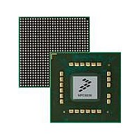
MPC8536DS Freescale Semiconductor, MPC8536DS Datasheet - Page 1252

MPC8536DS
Manufacturer Part Number
MPC8536DS
Description
BOARD DEV SYSTEM MPC8536E
Manufacturer
Freescale Semiconductor
Series
PowerQUICC III™r
Type
MPUr
Datasheets
1.MPC8536EBVTAVLA.pdf
(127 pages)
2.MPC8536EBVTAVLA.pdf
(1706 pages)
3.MPC8536DS.pdf
(2 pages)
4.MPC8536DS.pdf
(126 pages)
Specifications of MPC8536DS
Contents
Board, Software and Documentation
Processor Series
MPC85xx
Core
e500
Data Bus Width
32 bit
Maximum Clock Frequency
667 MHz
Operating Supply Voltage
- 0.3 V to + 1.21 V
Maximum Operating Temperature
+ 105 C
Data Ram Size
32 KB
Interface Type
SPI, USB
Program Memory Type
DDR2, DDR3, SDRAM
Core Size
32 Bit
Program Memory Size
544KB
Cpu Speed
1.5GHz
Digital Ic Case Style
BGA
No. Of Pins
783
Supply Voltage Range
0.95V To 1.05V
Rohs Compliant
Yes
For Use With/related Products
MPC8536
Lead Free Status / RoHS Status
Lead free / RoHS Compliant
- MPC8536EBVTAVLA PDF datasheet
- MPC8536EBVTAVLA PDF datasheet #2
- MPC8536DS PDF datasheet #3
- MPC8536DS PDF datasheet #4
- Current page: 1252 of 1706
- Download datasheet (15Mb)
SATA Controller
19.3.4.4
LinkCfg1, shown in
19-22
Offset 0x1_814C
Reset
25–16
15–8
Bit
7
6
5
4
3
2
1
0
W
R
31
TX_PRIM_JUNK
RX_BAD_CRC
TX_CONT_EN
TX_BAD_CRC
RX_SCR_EN
TX_SCR_EN
Link Layer Configuration Register1 (LinkCfg1)
EPNRT
Name
PRT
S4A
AR
MPC8536E PowerQUICC III Integrated Processor Reference Manual, Rev. 1
Figure
Figure 19-20. Link Layer Configuration Register1 (LinkCfg1)
PHY ready timer. These ten bits specify the timeout value of the PHY_READY timer. If
EN_PHY_TO is set, the link layer will count down on every rising edge of scanTxClk, as long
as PHY_READY is de-asserted. When the counter reaches 0, a PHY_RESET will be issued
to the PHY to try and re-establish communications with the far end. The timer is initially loaded
with a value equal to the concatenation of {PHY_READY_TIMER, 9b0_0000_0000}.
Align insertion rate. The SATA specification requires that the link layer send a pair of ALIGN
primitives at least every 254 words of data. This is achieved by setting ALIGN_RATE to
‘11111111’. However, for test purposes it is possible to send ALIGNs at a higher rate. This can
be achieved by setting ALIGN_RATE to a lower value (that is, ALIGN_RATE-1); words will be
sent by the link layer between each set of ALIGN primitive pairs.
Note: If SEND_4_ALIGNS is set, one should not set the ALIGN_RATE to be four or less. If
Enable PHY not ready timer. If PHY_READY is de-asserted for a length of time, as specified
by CFG_PHY_READY_TIMER, then this bit, when asserted, enables the link layer to re-issue
a PHY_RESET, thereby re-initiating OOB.
Send four ALIGNs. When asserted, four ALIGN primitives are transmitted at the specified rate,
instead of the normal two ALIGNS.
Rx scramble enable. If this bit is asserted, then descrambling of the receive data is enabled as
per the SATA specification.
Tx scramble enable. If this bit is asserted, then scrambling of the transmit data is enabled as
per the SATA specification.
TX prim junk. If this bit is de-asserted, then scrambled junk data is sent after a CONT primitive,
as per the SATA specification. If this bit is asserted, then the single character 0xDEADBEEF
is sent continuously instead. This is to aid debug.
TX CONT. If this bit is asserted, then the transmission of CONT primitives is enabled. If
de-asserted, then long sequences of repeated primitives can be sent by the link layer.
RX bad CRC. When a rising edge is detected on this bit, it causes a bad CRC to be detected
for the current frame. This bit has to be toggled from a 0 to a 1 to enable this feature.
Tx bad CRC. A bad CRC (inverted value of the correct CRC) value will be transmitted for one
FIS only by the link layer when a rising edge is detected on this signal. This bit has to be
toggled from a 0 to a 1 to enable this feature.
Table 19-19. LinkCfg Field Descriptions (continued)
19-20, controls the configuration of the link layer.
SEND_4_ALIGNS is not set, one should not set the ALIGN_RATE to be two or less.
—
All zeros
Description
7
CD PRIM_OVR_STATE
Freescale Semiconductor
6
5
Access: Read/Write
0
Related parts for MPC8536DS
Image
Part Number
Description
Manufacturer
Datasheet
Request
R
Part Number:
Description:
Manufacturer:
Freescale Semiconductor, Inc
Datasheet:
Part Number:
Description:
Manufacturer:
Freescale Semiconductor, Inc
Datasheet:
Part Number:
Description:
Manufacturer:
Freescale Semiconductor, Inc
Datasheet:
Part Number:
Description:
Manufacturer:
Freescale Semiconductor, Inc
Datasheet:
Part Number:
Description:
Manufacturer:
Freescale Semiconductor, Inc
Datasheet:
Part Number:
Description:
Manufacturer:
Freescale Semiconductor, Inc
Datasheet:
Part Number:
Description:
Manufacturer:
Freescale Semiconductor, Inc
Datasheet:
Part Number:
Description:
Manufacturer:
Freescale Semiconductor, Inc
Datasheet:
Part Number:
Description:
Manufacturer:
Freescale Semiconductor, Inc
Datasheet:
Part Number:
Description:
Manufacturer:
Freescale Semiconductor, Inc
Datasheet:
Part Number:
Description:
Manufacturer:
Freescale Semiconductor, Inc
Datasheet:
Part Number:
Description:
Manufacturer:
Freescale Semiconductor, Inc
Datasheet:
Part Number:
Description:
Manufacturer:
Freescale Semiconductor, Inc
Datasheet:
Part Number:
Description:
Manufacturer:
Freescale Semiconductor, Inc
Datasheet:
Part Number:
Description:
Manufacturer:
Freescale Semiconductor, Inc
Datasheet:


