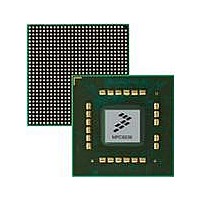
MPC8536DS Freescale Semiconductor, MPC8536DS Datasheet - Page 1592

MPC8536DS
Manufacturer Part Number
MPC8536DS
Description
BOARD DEV SYSTEM MPC8536E
Manufacturer
Freescale Semiconductor
Series
PowerQUICC III™r
Type
MPUr
Datasheets
1.MPC8536EBVTAVLA.pdf
(127 pages)
2.MPC8536EBVTAVLA.pdf
(1706 pages)
3.MPC8536DS.pdf
(2 pages)
4.MPC8536DS.pdf
(126 pages)
Specifications of MPC8536DS
Contents
Board, Software and Documentation
Processor Series
MPC85xx
Core
e500
Data Bus Width
32 bit
Maximum Clock Frequency
667 MHz
Operating Supply Voltage
- 0.3 V to + 1.21 V
Maximum Operating Temperature
+ 105 C
Data Ram Size
32 KB
Interface Type
SPI, USB
Program Memory Type
DDR2, DDR3, SDRAM
Core Size
32 Bit
Program Memory Size
544KB
Cpu Speed
1.5GHz
Digital Ic Case Style
BGA
No. Of Pins
783
Supply Voltage Range
0.95V To 1.05V
Rohs Compliant
Yes
For Use With/related Products
MPC8536
Lead Free Status / RoHS Status
Lead free / RoHS Compliant
- MPC8536EBVTAVLA PDF datasheet
- MPC8536EBVTAVLA PDF datasheet #2
- MPC8536DS PDF datasheet #3
- MPC8536DS PDF datasheet #4
- Current page: 1592 of 1706
- Download datasheet (15Mb)
Debug Features and Watchpoint Facility
25.3.1
The following sections describe the control registers for the watchpoint monitor facility.
25.3.1.1
The watchpoint monitor control registers (WMCR0, WMCR1) shown in
control the specification of watchpoint monitor events.
25-10
0xE_200C WMAR—Watchpoint monitor address register
0xE_201C WMSR—Watchpoint monitor status register
0xE_204C TBAR—Trace buffer address register
0xE_205C TBSR—Trace buffer status register
0xE_20A0 PCIDR—Programmed context ID register
0xE_20A4 CCIDR—Current context ID register
0xE_20B0 TOSR—Trigger output source register
0xE_2014
0xE_2018
0xE_2040
0xE_2044
0xE_2054
0xE_2058
0xE_2060
0xE_2064
0xE_2068
Offset 0x000
Reset
Memory
Offset
Local
W
R
EN AMD TMD ECEN NECEN SIDEN TIDEN
0
WMAMR—Watchpoint monitor address mask register
WMTMR—Watchpoint monitor transaction mask register
TBCR0—Trace buffer control register 0
TBCR1—Trace buffer control register 1
TBAMR—Trace buffer address mask register
TBTMR—Trace buffer transaction mask register
TBACR—Trace buffer access control register
TBADHR—Trace buffer access data high register
TBADR—Trace buffer access data register
Watchpoint Monitor Register Descriptions
1
Watchpoint Monitor Control Registers 0–1 (WMCR0, WMCR1)
2
Table 25-6. Debug and Watchpoint Monitor Memory Map (continued)
MPC8536E PowerQUICC III Integrated Processor Reference Manual, Rev. 1
Figure 25-2. Watchpoint Monitor Control Register 0 (WMCR0)
3
4
Register
5
Trace Buffer Registers
Context ID Registers
6
Other Registers
7
All zeros
—
Access
R/W
R/W
R/W
R/W
R/W
R/W
R/W
R/W
R/W
R/W
R/W
R/W
R/W
R/W
R/W
R/W
Figure 25-2
0x0000_0000
0x0000_0000
0x0000_0000
0x0000_0000
0x0000_0000
0x0000_0000
0x0000_0000
0x0000_0000
0x0000_0000
0x0000_0000
0x0000_0000
0x0000_0000
0x0000_0000
0x0000_0000
0x0000_0000
0x0000_0000
20 21
Reset
STRT
Freescale Semiconductor
23 24
and
Access: Read/Write
Figure 25-3
25.3.1.2/25-12
25.3.1.3/25-13
25.3.1.4/25-13
25.3.1.5/25-15
25.3.2.1/25-15
25.3.2.1/25-15
25.3.2.2/25-18
25.3.2.3/25-18
25.3.2.4/25-19
25.3.2.5/25-19
25.3.2.6/25-20
25.3.2.7/25-21
25.3.2.8/25-21
25.3.3.1/25-22
25.3.3.2/25-23
25.3.4.1/25-23
Section/Page
—
31
Related parts for MPC8536DS
Image
Part Number
Description
Manufacturer
Datasheet
Request
R
Part Number:
Description:
Manufacturer:
Freescale Semiconductor, Inc
Datasheet:
Part Number:
Description:
Manufacturer:
Freescale Semiconductor, Inc
Datasheet:
Part Number:
Description:
Manufacturer:
Freescale Semiconductor, Inc
Datasheet:
Part Number:
Description:
Manufacturer:
Freescale Semiconductor, Inc
Datasheet:
Part Number:
Description:
Manufacturer:
Freescale Semiconductor, Inc
Datasheet:
Part Number:
Description:
Manufacturer:
Freescale Semiconductor, Inc
Datasheet:
Part Number:
Description:
Manufacturer:
Freescale Semiconductor, Inc
Datasheet:
Part Number:
Description:
Manufacturer:
Freescale Semiconductor, Inc
Datasheet:
Part Number:
Description:
Manufacturer:
Freescale Semiconductor, Inc
Datasheet:
Part Number:
Description:
Manufacturer:
Freescale Semiconductor, Inc
Datasheet:
Part Number:
Description:
Manufacturer:
Freescale Semiconductor, Inc
Datasheet:
Part Number:
Description:
Manufacturer:
Freescale Semiconductor, Inc
Datasheet:
Part Number:
Description:
Manufacturer:
Freescale Semiconductor, Inc
Datasheet:
Part Number:
Description:
Manufacturer:
Freescale Semiconductor, Inc
Datasheet:
Part Number:
Description:
Manufacturer:
Freescale Semiconductor, Inc
Datasheet:


