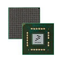
MPC8536DS Freescale Semiconductor, MPC8536DS Datasheet - Page 663

MPC8536DS
Manufacturer Part Number
MPC8536DS
Description
BOARD DEV SYSTEM MPC8536E
Manufacturer
Freescale Semiconductor
Series
PowerQUICC III™r
Type
MPUr
Datasheets
1.MPC8536EBVTAVLA.pdf
(127 pages)
2.MPC8536EBVTAVLA.pdf
(1706 pages)
3.MPC8536DS.pdf
(2 pages)
4.MPC8536DS.pdf
(126 pages)
Specifications of MPC8536DS
Contents
Board, Software and Documentation
Processor Series
MPC85xx
Core
e500
Data Bus Width
32 bit
Maximum Clock Frequency
667 MHz
Operating Supply Voltage
- 0.3 V to + 1.21 V
Maximum Operating Temperature
+ 105 C
Data Ram Size
32 KB
Interface Type
SPI, USB
Program Memory Type
DDR2, DDR3, SDRAM
Core Size
32 Bit
Program Memory Size
544KB
Cpu Speed
1.5GHz
Digital Ic Case Style
BGA
No. Of Pins
783
Supply Voltage Range
0.95V To 1.05V
Rohs Compliant
Yes
For Use With/related Products
MPC8536
Lead Free Status / RoHS Status
Lead free / RoHS Compliant
- MPC8536EBVTAVLA PDF datasheet
- MPC8536EBVTAVLA PDF datasheet #2
- MPC8536DS PDF datasheet #3
- MPC8536DS PDF datasheet #4
- Current page: 663 of 1706
- Download datasheet (15Mb)
Table 13-10
13.3.1.4
The UPM machine mode registers (MAMR, MBMR and MCMR), shown in
configuration for the three UPMs.
Offset MAMR: 0x0_5070
Table 13-11
Freescale Semiconductor
Reset
Reset
0–31
Bits
Bits
2–3
W
W
0
1
4
R
R
MBMR: 0x0_5074
MCMR: 0x0_5078
—
16
0
UWPL LUPWAIT polarity active low. Sets the polarity of the LUPWAIT pin when in UPM mode.
Name
Name
RFEN Refresh enable. Indicates that the UPM needs refresh services. This bit must be set for UPMA (refresh
RLF
OP
—
A
RFEN
describes UPM mode fields.
describes the MAR fields.
UPM Mode Registers (M x MR)
17
1
Address that can be output to the address signals under control of the AMX bits in the UPM RAM word.
Reserved
executor) if refresh services are required on any UPM assigned chip selects. If MAMR[RFEN] = 0, no refresh
services can be provided, even if UPMB and/or UPMC have their RFEN bit set.
0 Refresh services are not required
1 Refresh services are required
Command opcode. Determines the command executed by the UPM n when a memory access hits a UPM
assigned bank.
00 Normal operation
01 Write to UPM array. On the next memory access that hits a UPM assigned bank, write the contents of the
10 Read from UPM array. On the next memory access that hits a UPM assigned bank, read the contents of
11 Run pattern. On the next memory access that hits a UPM assigned bank, run the pattern written in the
0 LUPWAIT is active high.
1 LUPWAIT is active low.
MDR into the RAM location pointed to by MAD. After the access, MAD is automatically incremented.
the RAM location pointed to by MAD into the MDR. After the access, MAD is automatically incremented.
RAM array. The pattern run starts at the location pointed to by MAD and continues until the LAST bit is
set in the RAM word.
MPC8536E PowerQUICC III Integrated Processor Reference Manual, Rev. 1
18
2
OP
3
WLF
UWPL
Figure 13-7. UPM Mode Registers (M x MR)
4
Table 13-11. M x MR Field Descriptions
Table 13-10. MAR Field Descriptions
21
5
AM
22
7
All zeros
All zeros
TLF
Description
Description
8
DS
25
9
10
26
G0CL
Figure
12
Enhanced Local Bus Controller
MAD
13-7, contain the
GPL4
13
Access: Read/Write
14
RLF
13-21
15
31
Related parts for MPC8536DS
Image
Part Number
Description
Manufacturer
Datasheet
Request
R
Part Number:
Description:
Manufacturer:
Freescale Semiconductor, Inc
Datasheet:
Part Number:
Description:
Manufacturer:
Freescale Semiconductor, Inc
Datasheet:
Part Number:
Description:
Manufacturer:
Freescale Semiconductor, Inc
Datasheet:
Part Number:
Description:
Manufacturer:
Freescale Semiconductor, Inc
Datasheet:
Part Number:
Description:
Manufacturer:
Freescale Semiconductor, Inc
Datasheet:
Part Number:
Description:
Manufacturer:
Freescale Semiconductor, Inc
Datasheet:
Part Number:
Description:
Manufacturer:
Freescale Semiconductor, Inc
Datasheet:
Part Number:
Description:
Manufacturer:
Freescale Semiconductor, Inc
Datasheet:
Part Number:
Description:
Manufacturer:
Freescale Semiconductor, Inc
Datasheet:
Part Number:
Description:
Manufacturer:
Freescale Semiconductor, Inc
Datasheet:
Part Number:
Description:
Manufacturer:
Freescale Semiconductor, Inc
Datasheet:
Part Number:
Description:
Manufacturer:
Freescale Semiconductor, Inc
Datasheet:
Part Number:
Description:
Manufacturer:
Freescale Semiconductor, Inc
Datasheet:
Part Number:
Description:
Manufacturer:
Freescale Semiconductor, Inc
Datasheet:
Part Number:
Description:
Manufacturer:
Freescale Semiconductor, Inc
Datasheet:


