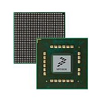
MPC8536DS Freescale Semiconductor, MPC8536DS Datasheet - Page 1097

MPC8536DS
Manufacturer Part Number
MPC8536DS
Description
BOARD DEV SYSTEM MPC8536E
Manufacturer
Freescale Semiconductor
Series
PowerQUICC III™r
Type
MPUr
Datasheets
1.MPC8536EBVTAVLA.pdf
(127 pages)
2.MPC8536EBVTAVLA.pdf
(1706 pages)
3.MPC8536DS.pdf
(2 pages)
4.MPC8536DS.pdf
(126 pages)
Specifications of MPC8536DS
Contents
Board, Software and Documentation
Processor Series
MPC85xx
Core
e500
Data Bus Width
32 bit
Maximum Clock Frequency
667 MHz
Operating Supply Voltage
- 0.3 V to + 1.21 V
Maximum Operating Temperature
+ 105 C
Data Ram Size
32 KB
Interface Type
SPI, USB
Program Memory Type
DDR2, DDR3, SDRAM
Core Size
32 Bit
Program Memory Size
544KB
Cpu Speed
1.5GHz
Digital Ic Case Style
BGA
No. Of Pins
783
Supply Voltage Range
0.95V To 1.05V
Rohs Compliant
Yes
For Use With/related Products
MPC8536
Lead Free Status / RoHS Status
Lead free / RoHS Compliant
- MPC8536EBVTAVLA PDF datasheet
- MPC8536EBVTAVLA PDF datasheet #2
- MPC8536DS PDF datasheet #3
- MPC8536DS PDF datasheet #4
- Current page: 1097 of 1706
- Download datasheet (15Mb)
Chapter 17
PCI Express Interface Controller
The PCI Express interface is compatible with the PCI Express™ Base Specification, Revision 1.0a
(available from http://www.pcisig.org). It is beyond the scope of this manual to document the intricacies
of the PCI Express protocol. This chapter describes the PCI Express controller of this device and provides
a basic description of the PCI Express protocol. The specific emphasis is directed at how the device
implements the PCI Express specification. Designers of systems incorporating PCI Express devices should
refer to the specification for a thorough description of PCI Express.
17.1
The PCI Express controller provides the mechanism to communicate with PCI Express devices.
Figure 17-1
17.1.1
The PCI Express controller connects the internal platform to a 2.5- GHz serial interface. The MPC8536E
offers one, two, or three PCI Express interfaces with up to x8 link width. (Note that the x8 link width is
only available at CCB clock rates of 527 MHz or greater.)
As both an initiator and a target device, the PCI Express interface is capable of high-bandwidth data
transfer and is designed to support next generation I/O devices. Upon coming out of reset, the PCI Express
interface performs link width negotiation and exchanges flow control credits with its link partner. Once
link autonegotiation is successful, the controller is in operation.
Internally, the design contains queues to keep track of inbound and outbound transactions. There is control
logic that handles buffer management, bus protocol, transaction spawning and tag generation. In addition,
there are memory blocks used to store inbound and outbound data.
The PCI Express controller can be configured to operate as either a PCI Express root complex (RC) or an
endpoint (EP) device. An RC device connects the host CPU/memory subsystem to I/O devices while an
EP device typically denotes a peripheral or I/O device. In RC mode, a PCI Express type 1 configuration
header is used; in EP mode, a PCI Express type 0 configuration header is used.
Freescale Semiconductor
Introduction
Overview
is a high-level block diagram of the PCI Express controller.
Much of the available PCI Express literature refers to a 16-bit quantity as a
WORD and a 32-bit quantity as a DWORD. Note that this is inconsistent
with the terminology in the rest of this manual where the terms ‘word’ and
‘double word’ refer to a 32-bit and 64-bit quantity, respectively. Where
necessary to avoid confusion, the precise number of bits or bytes is
specified.
MPC8536E PowerQUICC III Integrated Processor Reference Manual, Rev. 1
NOTE
17-1
Related parts for MPC8536DS
Image
Part Number
Description
Manufacturer
Datasheet
Request
R
Part Number:
Description:
Manufacturer:
Freescale Semiconductor, Inc
Datasheet:
Part Number:
Description:
Manufacturer:
Freescale Semiconductor, Inc
Datasheet:
Part Number:
Description:
Manufacturer:
Freescale Semiconductor, Inc
Datasheet:
Part Number:
Description:
Manufacturer:
Freescale Semiconductor, Inc
Datasheet:
Part Number:
Description:
Manufacturer:
Freescale Semiconductor, Inc
Datasheet:
Part Number:
Description:
Manufacturer:
Freescale Semiconductor, Inc
Datasheet:
Part Number:
Description:
Manufacturer:
Freescale Semiconductor, Inc
Datasheet:
Part Number:
Description:
Manufacturer:
Freescale Semiconductor, Inc
Datasheet:
Part Number:
Description:
Manufacturer:
Freescale Semiconductor, Inc
Datasheet:
Part Number:
Description:
Manufacturer:
Freescale Semiconductor, Inc
Datasheet:
Part Number:
Description:
Manufacturer:
Freescale Semiconductor, Inc
Datasheet:
Part Number:
Description:
Manufacturer:
Freescale Semiconductor, Inc
Datasheet:
Part Number:
Description:
Manufacturer:
Freescale Semiconductor, Inc
Datasheet:
Part Number:
Description:
Manufacturer:
Freescale Semiconductor, Inc
Datasheet:
Part Number:
Description:
Manufacturer:
Freescale Semiconductor, Inc
Datasheet:


