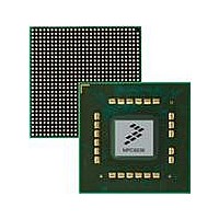
MPC8536DS Freescale Semiconductor, MPC8536DS Datasheet - Page 1190

MPC8536DS
Manufacturer Part Number
MPC8536DS
Description
BOARD DEV SYSTEM MPC8536E
Manufacturer
Freescale Semiconductor
Series
PowerQUICC III™r
Type
MPUr
Datasheets
1.MPC8536EBVTAVLA.pdf
(127 pages)
2.MPC8536EBVTAVLA.pdf
(1706 pages)
3.MPC8536DS.pdf
(2 pages)
4.MPC8536DS.pdf
(126 pages)
Specifications of MPC8536DS
Contents
Board, Software and Documentation
Processor Series
MPC85xx
Core
e500
Data Bus Width
32 bit
Maximum Clock Frequency
667 MHz
Operating Supply Voltage
- 0.3 V to + 1.21 V
Maximum Operating Temperature
+ 105 C
Data Ram Size
32 KB
Interface Type
SPI, USB
Program Memory Type
DDR2, DDR3, SDRAM
Core Size
32 Bit
Program Memory Size
544KB
Cpu Speed
1.5GHz
Digital Ic Case Style
BGA
No. Of Pins
783
Supply Voltage Range
0.95V To 1.05V
Rohs Compliant
Yes
For Use With/related Products
MPC8536
Lead Free Status / RoHS Status
Lead free / RoHS Compliant
- MPC8536EBVTAVLA PDF datasheet
- MPC8536EBVTAVLA PDF datasheet #2
- MPC8536DS PDF datasheet #3
- MPC8536DS PDF datasheet #4
- Current page: 1190 of 1706
- Download datasheet (15Mb)
PCI Express Interface Controller
The fields of the PCI Express power management timer register are described in
17.3.10.16 PCI Express PME Time-Out Register (EP-Mode Only)—0x454
The PCI Express PME time-out register, shown in
that the controller uses before re-sending a PME message to the host. If PME is requested by a function
and the host does not clear the associated PME_STAT bit even after this time-out has expired, the PME
message is sent again to the host by the PCI Express controller. This register is supported only for EP
mode.
The fields of the PCI Express PME time-out register are described in
17-94
31–24
23–12 L1_WAIT_PERIOD Wait period (in PCI Express controller core clock cycles) before entering L1 power state after all
31–26
11–0
25–0
Offset 0x454 (EP-mode only)
Bits
Reset 0
Bits
W
R
31
PME_TIMEOUT
L0s_TIME_IN
0
Name
Name
0
—
—
—
Figure 17-117. PCI Express PME Time-Out Register (PEX_PME_TIMEOUT)
0
MPC8536E PowerQUICC III Integrated Processor Reference Manual, Rev. 1
0
26 25
0
Reserved
functions are in a non-D0 power state. The value is calculated as:
The time value must be less than 2 µsec; the default value (0x14D) is 1 µsec for the default clock
frequency of 333 MHz.
Time in value (in PCI Express controller core clock cycles) for entering L0s power state. The
value is calculated as:
The maximum time value is 7 µsec; the default value (0x7CE) is 6 µsec for the default clock
frequency of 333 MHz.
Reserved
The PME time-out value specifies the interval before PME messages are resent by the
controller, provided the PME_STAT bit in the PCI Express power management status and
control register (offset 0x48) is not cleared by the host. The value for PME_TIMEOUT is
specified in terms of PCI Express controller core clock cycles. The value is calculated as:
The minimum time value is 100 msec; the default value (0x1FC1E20) is 100 msec for the default
clock frequency of 333 MHz.
Table 17-114. PEX_PME_TIMEOUT Field Descriptions
0
Time (in µsec) × PCI Express controller core clock frequency (in MHz)
Time (in µsec) × PCI Express controller core clock frequency (in MHz)
Time (in µsec) × PCI Express controller core clock frequency (in MHz)
Table 17-113. PEX_PM_TIMER Field Descriptions
1
1
1
1
1
1
1
0
Figure
0
0
PME_TIMEOUT
17-117, is used to program the time-out value
Description
Description
0
0
1
1
Table
1
1
17-113.
0
0
Table
0
Freescale Semiconductor
1
Access: Read/Write
17-113.
0
0
0
0
0
0
Related parts for MPC8536DS
Image
Part Number
Description
Manufacturer
Datasheet
Request
R
Part Number:
Description:
Manufacturer:
Freescale Semiconductor, Inc
Datasheet:
Part Number:
Description:
Manufacturer:
Freescale Semiconductor, Inc
Datasheet:
Part Number:
Description:
Manufacturer:
Freescale Semiconductor, Inc
Datasheet:
Part Number:
Description:
Manufacturer:
Freescale Semiconductor, Inc
Datasheet:
Part Number:
Description:
Manufacturer:
Freescale Semiconductor, Inc
Datasheet:
Part Number:
Description:
Manufacturer:
Freescale Semiconductor, Inc
Datasheet:
Part Number:
Description:
Manufacturer:
Freescale Semiconductor, Inc
Datasheet:
Part Number:
Description:
Manufacturer:
Freescale Semiconductor, Inc
Datasheet:
Part Number:
Description:
Manufacturer:
Freescale Semiconductor, Inc
Datasheet:
Part Number:
Description:
Manufacturer:
Freescale Semiconductor, Inc
Datasheet:
Part Number:
Description:
Manufacturer:
Freescale Semiconductor, Inc
Datasheet:
Part Number:
Description:
Manufacturer:
Freescale Semiconductor, Inc
Datasheet:
Part Number:
Description:
Manufacturer:
Freescale Semiconductor, Inc
Datasheet:
Part Number:
Description:
Manufacturer:
Freescale Semiconductor, Inc
Datasheet:
Part Number:
Description:
Manufacturer:
Freescale Semiconductor, Inc
Datasheet:


