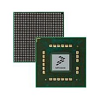
MPC8536DS Freescale Semiconductor, MPC8536DS Datasheet - Page 1703

MPC8536DS
Manufacturer Part Number
MPC8536DS
Description
BOARD DEV SYSTEM MPC8536E
Manufacturer
Freescale Semiconductor
Series
PowerQUICC III™r
Type
MPUr
Datasheets
1.MPC8536EBVTAVLA.pdf
(127 pages)
2.MPC8536EBVTAVLA.pdf
(1706 pages)
3.MPC8536DS.pdf
(2 pages)
4.MPC8536DS.pdf
(126 pages)
Specifications of MPC8536DS
Contents
Board, Software and Documentation
Processor Series
MPC85xx
Core
e500
Data Bus Width
32 bit
Maximum Clock Frequency
667 MHz
Operating Supply Voltage
- 0.3 V to + 1.21 V
Maximum Operating Temperature
+ 105 C
Data Ram Size
32 KB
Interface Type
SPI, USB
Program Memory Type
DDR2, DDR3, SDRAM
Core Size
32 Bit
Program Memory Size
544KB
Cpu Speed
1.5GHz
Digital Ic Case Style
BGA
No. Of Pins
783
Supply Voltage Range
0.95V To 1.05V
Rohs Compliant
Yes
For Use With/related Products
MPC8536
Lead Free Status / RoHS Status
Lead free / RoHS Compliant
- MPC8536EBVTAVLA PDF datasheet
- MPC8536EBVTAVLA PDF datasheet #2
- MPC8536DS PDF datasheet #3
- MPC8536DS PDF datasheet #4
- Current page: 1703 of 1706
- Download datasheet (15Mb)
Index
Freescale Semiconductor
DDR
DMA
DUART
eTSEC
figure showing groupings, 3-1
output signal states at power-on reset, 3-17
reference by functional block, 3-2
MA[0:14] (address bus), 8-7
MBA[0:1] (logical bank address), 8-7
MCAS (column address strobe), 8-8
MCK[0:5] (DDR clock output complements), 8-10
MCK[0:5] (DDR clock outputs), 8-10
MCKE[0:3] (DDR clock enables), 8-10
MCS[0:3] (chip selects), 8-8
MDIC[0:1] (driver impedance calibration), 8-9
MDM[0:8] (SDRAM data output mask), 8-9
MDQS[0:8] (data bus strobes), 8-6, 8-61
MDVAL (debug mode data valid), 4-23, 25-3, 25-6
MECC[0:5] (error correcting code)
MECC[0:7] (error correcting code), 4-23, 8-7
MODT[0:3] (on-die termination), 8-9
MRAS (row address strobe), 8-8
MSRCID[0:4] (debug source ID), 4-23, 25-3, 25-7
MWE (write enable), 8-8, 8-9
DMA_DACK[0:3] (DMA acknowledge), 15-5
DMA_DDONE[0:3] (DMA done), 15-5
DMA_DREQ[0:3] (DMA request), 15-5
UART_CTS[0:1] (DUART clear to send), 12-1, 12-3
UART_RTS[0:1] (DUART request to send), 12-1, 12-3
UART_SIN [0:1] (DUART transmitter serial data in),
UART_SOUT [0:1] (DUART transmitter serial data
EC_GTX_CLK125 (eTSEC gigabit transmit 125 MHz
EC_MDC (eTSEC management data clock), 14-11
EC_MDIO (eTSEC management data input/output,
FIFO interface signal summary, 14-159
TSECn_COL (eTSEC 1–4 collision input), 14-10
TSECn_CRS (eTSEC 1–4 carrier sense input/FIFO
TSECn_GTX_CLK (eTSEC 1–4 gigabit transmit clock),
TSECn_RX_CLK (eTSEC 1–4 receive clock), 14-11
TSECn_RX_DV (eTSEC 1–4 receive data valid), 14-11
TSECn_RX_ER (eTSEC 1–4 receive error), 14-12
TSECn_RXD[7:0] (eTSEC 1–4 receive data in), 14-12
TSECn_TX_CLK (eTSEC 1–4 transmit clock in), 14-12
TSECn_TX_EN (eTSEC 1–4 transmit data valid), 14-13
see also Power-on reset (POR)
as debug signals, 25-3, 25-7
12-2, 12-3
out), 12-2, 12-3
source), 14-11
BIDI), 14-11
receiver flow control), 14-10
14-10
MPC8536E PowerQUICC III Integrated Processor Reference Manual, Rev. 1
global utilities
GPIO, 22-2
I
JTAG
LBC
other
PCI Express
PCI/PCI-X
2
C
TSECn_TX_ER (eTSEC 1–4 transmit error), 14-13
TSECn_TXD[7:0] (eTSEC 1–4 transmit data out), 14-13
ASLEEP, 23-2
CKSTP_IN (checkstop in), 23-2
CKSTP_OUT (checkstop out), 23-3
CLK_OUT, 23-3, 23-33
SCL (serial clock), 11-3, 11-4
SDA (serial data), 11-3, 11-4
TCK (JTAG test clock), 25-8
TDI (JTAG test data input), 25-8
TDO (JTAG test data output), 25-8
TMS (JTAG test mode select), 25-8
TRST (JTAG test reset), 25-9
LA[27:31] (non-multiplexed address), 13-7
LAD[0:31] (multiplexed address/data), 13-7
LALE (external address latch enable), 13-5, 13-43
LBCTL (data buffer control), 13-7, 13-46
LBS[0:3] (UPM byte select), 13-6
LCK[0:2] (clock), 13-8
LCS[0:7] (chip select), 13-6
LCS0 (LBC chip select 0), 13-58, 13-72
LDP[0:3] (data parity), 13-8
LGPL0 (GP line 0), 13-6
LGPL1 (GP line 1), 13-6
LGPL2 (GP line 2), 13-6
LGPL3 (GP line 3), 13-6
LGPL4 (GP line 4), 13-7
LGPL5 (GP line 5), 13-7
LGTA (GPCM transfer acknowledge), 13-7, 13-57
LOE (GPCM output enable), 13-6
LPBSE (parity byte select), 13-7
LSYNC_IN (DLL synchronization in), 13-8
LSYNC_OUT (DLL synchronization out), 13-8
LWE[0:3] (GPCM write enable), 13-6
MDVAL (debug mode data valid), 4-23, 13-8, 25-3, 25-6
MSRCID[0:4] (debug source ID), 4-23, 13-8, 25-3, 25-7
TA (data transfer acknowledge), 13-45
UPWAIT (UPM wait), 13-7, 13-75
TEST_SEL (factory test), 25-6
THERM[0:1] (thermal resistor access), 25-9
SD_RX[7:0]/SD_RX[7:0] (PCI Express serial data input
SD_TX[7:0]/SD_TX[7:0] (PCI Express serial data
and complement) signals, 17-5
output and complement) signals, 17-5
Index-17
S–S
Related parts for MPC8536DS
Image
Part Number
Description
Manufacturer
Datasheet
Request
R
Part Number:
Description:
Manufacturer:
Freescale Semiconductor, Inc
Datasheet:
Part Number:
Description:
Manufacturer:
Freescale Semiconductor, Inc
Datasheet:
Part Number:
Description:
Manufacturer:
Freescale Semiconductor, Inc
Datasheet:
Part Number:
Description:
Manufacturer:
Freescale Semiconductor, Inc
Datasheet:
Part Number:
Description:
Manufacturer:
Freescale Semiconductor, Inc
Datasheet:
Part Number:
Description:
Manufacturer:
Freescale Semiconductor, Inc
Datasheet:
Part Number:
Description:
Manufacturer:
Freescale Semiconductor, Inc
Datasheet:
Part Number:
Description:
Manufacturer:
Freescale Semiconductor, Inc
Datasheet:
Part Number:
Description:
Manufacturer:
Freescale Semiconductor, Inc
Datasheet:
Part Number:
Description:
Manufacturer:
Freescale Semiconductor, Inc
Datasheet:
Part Number:
Description:
Manufacturer:
Freescale Semiconductor, Inc
Datasheet:
Part Number:
Description:
Manufacturer:
Freescale Semiconductor, Inc
Datasheet:
Part Number:
Description:
Manufacturer:
Freescale Semiconductor, Inc
Datasheet:
Part Number:
Description:
Manufacturer:
Freescale Semiconductor, Inc
Datasheet:
Part Number:
Description:
Manufacturer:
Freescale Semiconductor, Inc
Datasheet:


